
Method of producing mechanical components of MEMS or nems structures made of monocrystalline silicon

Active Publication Date: 2009-07-02
COMMISSARIAT A LENERGIE ATOMIQUE ET AUX ENERGIES ALTERNATIVES
View PDF6 Cites 8 Cited by
  • Summary
  • Abstract
  • Description
  • Claims
  • Application Information

AI Technical Summary

Problems solved by technology

On the other hand, the major drawback of SOI technology is its high price.
Problems of poorly controlled stresses in the SOI have also recently been observed which, in certain configurations, are very detrimental to MEMS / NEMS.
Isotropic etching of SiGe is quite poorly selective compared to silicon, thereby limiting the technique to releases of narrow patterns (typically below one μm).
The thickness of silicon epitaxied on the SiGe is generally limited to several hundreds of nanometres (dislocations risk appearing if it is wished to obtain high silicon thicknesses).
This results in the creation of significant mechanical stress on the MEMS (due to the presence of the thermal oxide and metal on the released structures).
This addition of oxide and metal on the monocrystalline silicon renders the mechanical component less good (poorer quality factor in the case of a resonator for example).
This method is not very industrial and gives a very mediocre resolution of patterns.

Method used


Image

  • Method of producing mechanical components of MEMS or nems structures made of monocrystalline silicon
  • Method of producing mechanical components of MEMS or nems structures made of monocrystalline silicon
  • Method of producing mechanical components of MEMS or nems structures made of monocrystalline silicon

Examples


Embodiment Construction

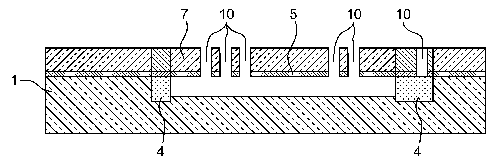
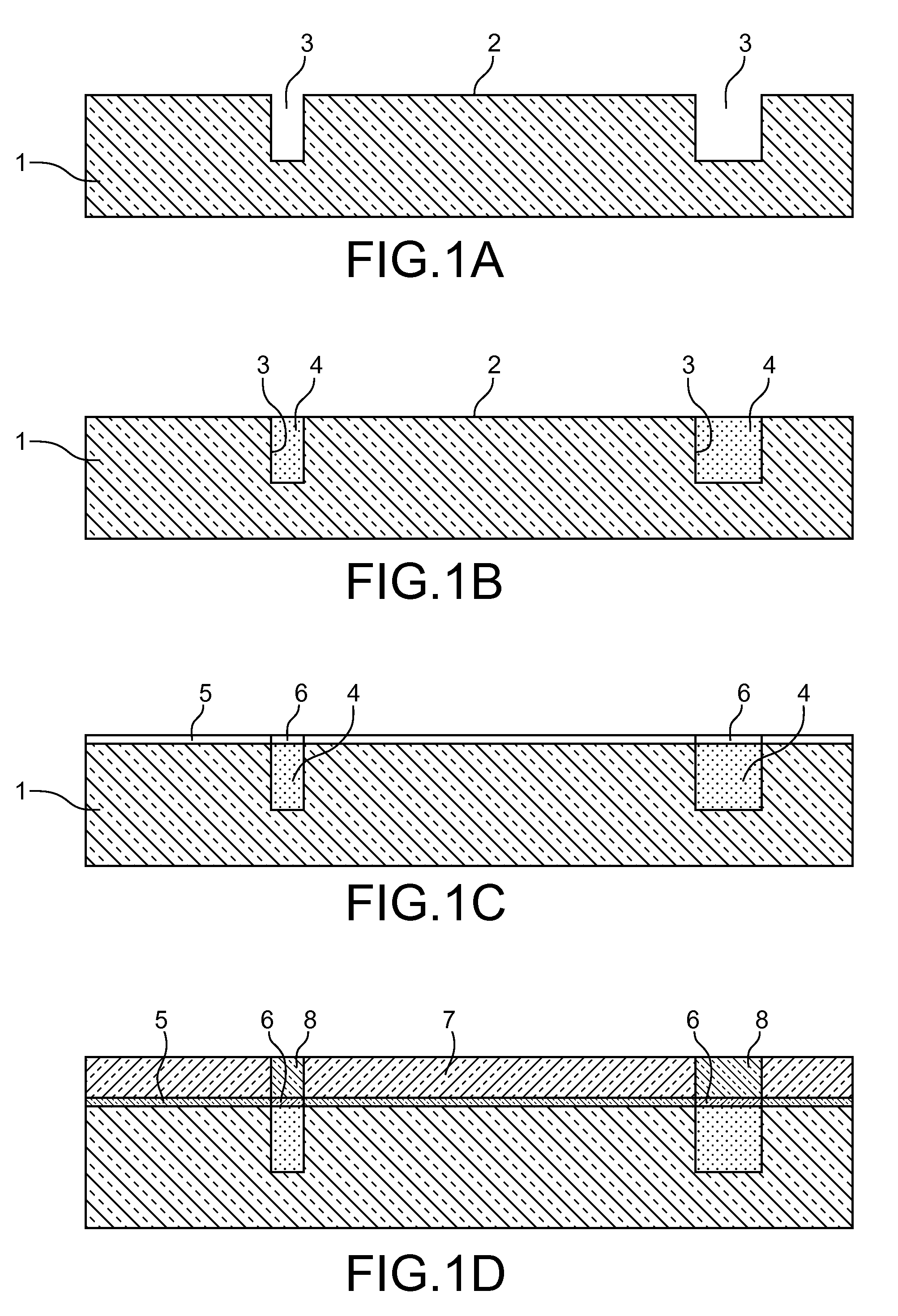
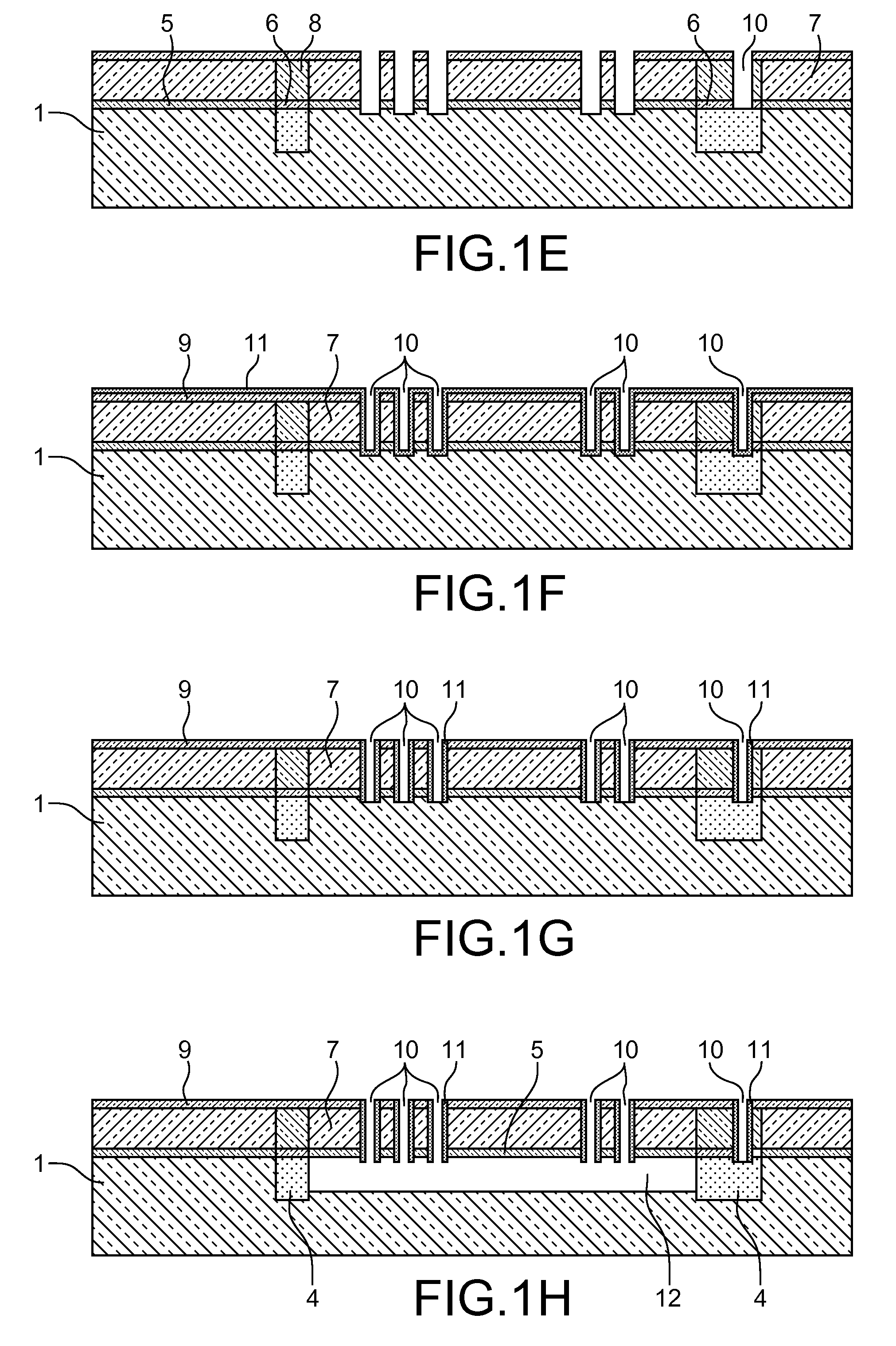
[0017]The present invention has been designed to overcome the abovementioned drawbacks of the prior art.

[0018]The method according to the invention may be used for all MEMS and NEMS applications. It uses a technology adapted to low cost and high volume markets: mobile telephony, automobiles, games, etc. By way of example, the following may be cited:[0019]for automobiles: accelerometers, gyrometers, pressure sensors, chemical sensors based on MEMS or NEMS mechanical resonators,[0020]for mobile telephony: time bases (RF resonators), MEMS or NEMS mechanical filters, accelerometers, microphones,[0021]for games: accelerometers, gyrometers.

[0022]The invention concerns a method of producing at least one mechanical component of MEMS or NEMS structure from a monocrystalline silicon substrate, comprising the steps of:

[0023]a) forming anchoring zones in one face of the substrate to delimit at least in part the mechanical component,

[0024]b) forming, on said face of the substrate, a lower protec...


PUM


Abstract

The invention concerns a method of producing at least one mechanical component of a MEMS or NEMS structure from a monocrystalline silicon substrate, comprising the steps of:forming anchoring zones in one face of the substrate to delimit the mechanical component,forming, on the face of the substrate, a lower protective layer made of material other than silicon and obtained by epitaxy from the face of the substrate,forming, on the lower protective layer, a silicon layer obtained by epitaxy from the lower protective layer,forming an upper protective layer on the silicon layer,etching the upper protective layer, the silicon layer and the lower protective layer, according to a pattern defining the mechanical component, until the substrate is reached and to provide access routes to the substrate,forming a protective layer on the walls formed by the etching of the pattern of the mechanical component in the epitaxied silicon layer,releasing the mechanical component by isotropic etching of the substrate from the access routes to the substrate, wherein said isotropic etching does not attack the lower and upper protective layers and the protective layer of the walls.

Description

TECHNICAL FIELD[0001]The invention relates to a method of producing mechanical components of MEMS (Micro-Electro-Mechanical System) or NEMS (Nano-Electro-Mechanical System) structures made of monocrystalline silicon. These structures are in particular used for the production of sensors and actuators.PRIOR ART[0002]The use of monocrystalline silicon for the formation of MEMS or NEMS components is interesting in several respects. Its mechanical properties are excellent, particularly compared to polycrystalline silicon. High thicknesses may be used (in the case of polycrystalline silicon, the thickness is generally limited to 20 μm). It has very good piezoelectric properties. Its semiconducting properties, well known and well controlled, enable a co-integration of these mechanical components with the associated electronics.[0003]In the prior art, there are three major ways of producing MEMS / NEMS structures made of monocrystalline silicon, in other words released mechanical components, ...

Claims


Application Information

Patent Timeline
IPC IPC(8): H01L21/00H01L21/71H01L21/31B82B1/00
CPCB81C1/00484B81C2201/053B81C1/00682
Inventor ROBERT, PHILIPPENGUYEN, VALERIE
Owner COMMISSARIAT A LENERGIE ATOMIQUE ET AUX ENERGIES ALTERNATIVES
Learn More