Method of forming stressed SOI FET having doped glass box layer using sacrificial stressed layer

a technology of glass box layer and stressed layer, which is applied in the field of semiconductor devices, can solve the problems of reducing the performance benefit to be gained from the soi structure, affecting the design flexibility of the transistor, and affecting the performance of the transistor,

Inactive Publication Date: 2011-02-15
ELPIS TECH INC
View PDF46 Cites 29 Cited by
  • Summary
  • Abstract
  • Description
  • Claims
  • Application Information

AI Technical Summary

Problems solved by technology

This fact hinders some of the flexibility of the design of the transistor to be formed thereon, as the underlying SiGe layer 14 can contribute to junction capacitance, reducing the performance benefit to be gained from the SOI structure.
In addition, the permanent presence of the SiGe layer 14 can lead to undesirable diffusion of germanium and arsenic into portions of the transistor to be formed in the active silicon region 12.
Another drawback is that threading defects can occur which can lead to shorts of the gate dielectric.

Method used


Image

  • Method of forming stressed SOI FET having doped glass box layer using sacrificial stressed layer
  • Method of forming stressed SOI FET having doped glass box layer using sacrificial stressed layer
  • Method of forming stressed SOI FET having doped glass box layer using sacrificial stressed layer

Examples


Embodiment Construction

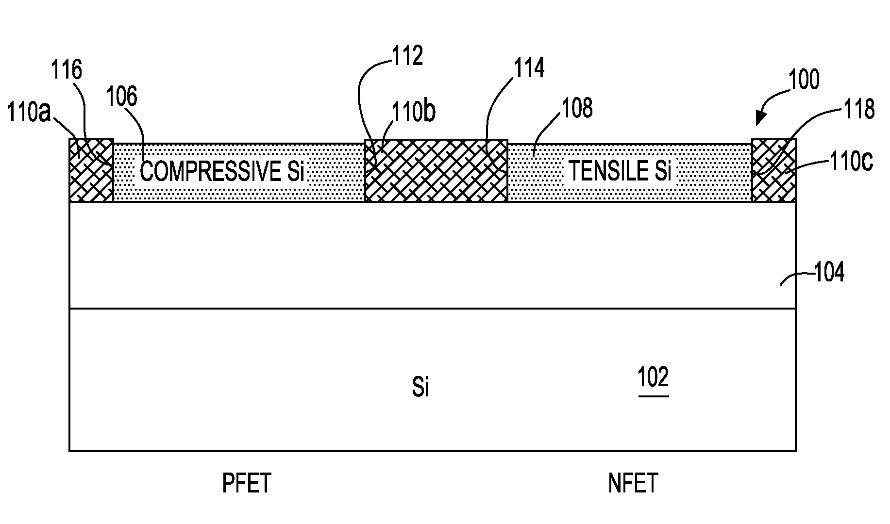
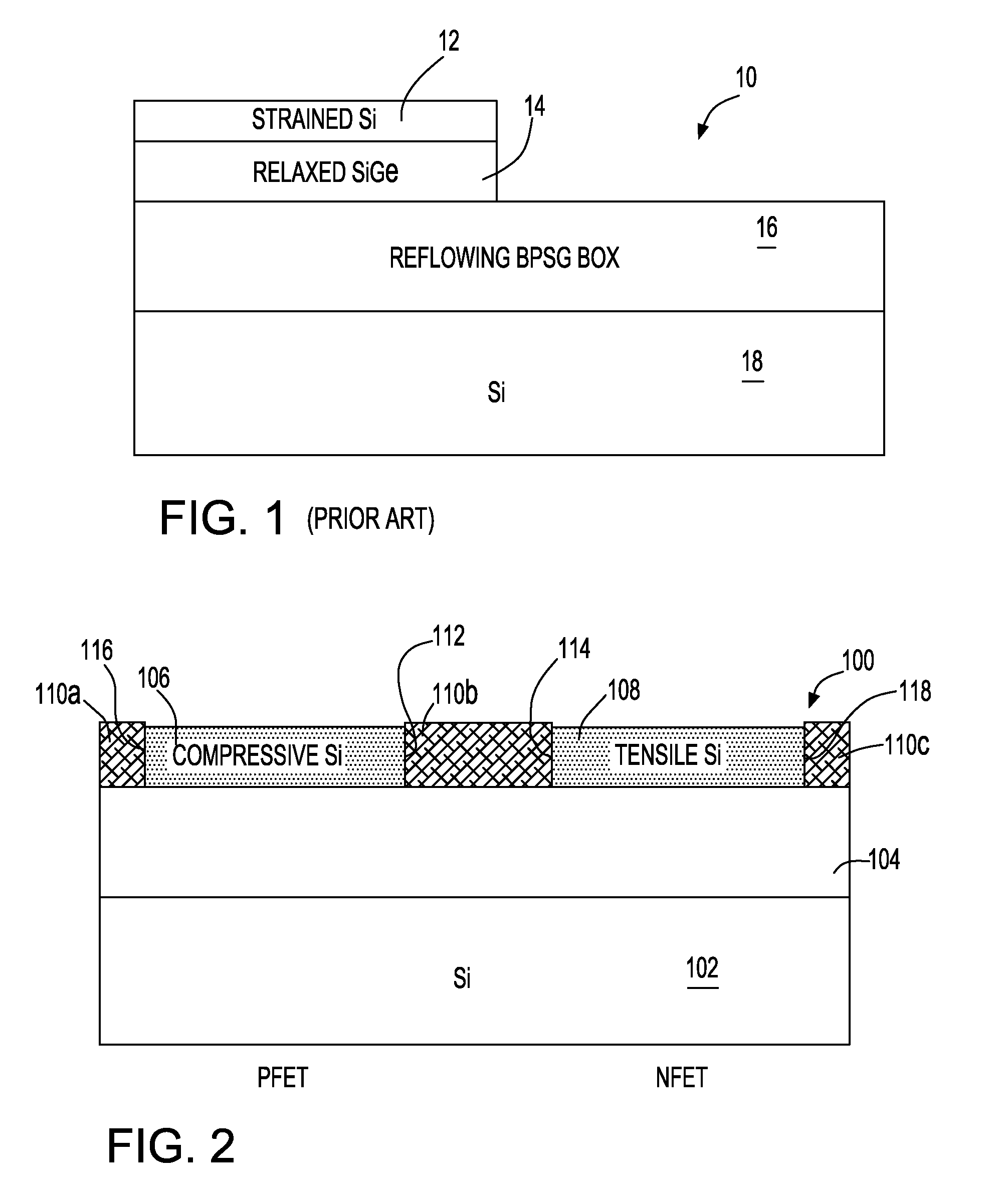
[0017]An SOI substrate 100 according to a first embodiment of the invention is illustrated in FIG. 2. As illustrated therein, the SOI substrate includes a bulk semiconductor region 102, over which a buried oxide (“BOX”) layer 104 is provided which includes doped silicate glass, for example borophosphosilicate glass (“BPSG”). The BOX layer consists essentially of doped silicate glass, and both boron and phosphorus dopants are dispersed typically throughout the layer, and typically evenly.

[0018]As further shown in FIG. 2, an SOI layer of the substrate includes a region 106 of compressive stressed monocrystalline silicon overlying the BOX layer 104. The SOI layer further includes a tensile stressed region 108 of monocrystalline silicon overlying the BOX layer 104. The BOX layer 104 separates the stressed silicon regions 106, 108 from the bulk semiconductor region 102. A trench isolation region 110b is disposed between peripheral edges 112, 114 of the two stressed silicon regions 106, 1...


PUM


Abstract

A method is provided for fabricating a semiconductor-on-insulator (“SOI”) substrate. In such method an SOI substrate is formed to include (i) an SOI layer of monocrystalline silicon separated from (ii) a bulk semiconductor layer by (iii) a buried oxide (“BOX”) layer including a layer of doped silicate glass. A sacrificial stressed layer is deposited onto the SOI substrate to overlie the SOI layer. Trenches are then etched through the sacrificial stressed layer and into the SOI layer. The SOI substrate is heated with the sacrificial stressed layer sufficiently to cause the glass layer to soften and the sacrificial stressed layer to relax, to thereby apply a stress to the SOI layer to form a stressed SOI layer. The trenches in the stressed SOI layer are then filled with a dielectric material to form trench isolation regions contacting peripheral edges of the stressed SOI layer, the trench isolation regions extending downwardly from a major surface of the stressed SOI layer towards the BOX layer. The sacrificial stressed layer is then removed to expose the stressed SOI layer. Field effect transistors can then be formed in the stressed SOI layer.

Description

BACKGROUND OF THE INVENTION[0001]The present invention relates to semiconductor devices and their fabrication. More particularly, the invention relates to preparation of a silicon-on-insulator (“SOI”) substrate in which at least a portion of the SOI substrate is stressed.[0002]Various methods exist for fabricating SOI substrates. In one particular example according to the prior art, illustrated in FIG. 1, an SOI substrate 10 is fabricated to contain a region of strained silicon 12 having tensile stress in which a transistor, for example, an n-type field effect transistor (“NFET”) will be formed. The tensile stressed silicon region 12 overlies a region 14 containing silicon germanium (SiGe) having relaxed stress, and the SiGe region, in turn, overlies a bulk silicon region 18, as separated therefrom by a buried oxide (“BOX”) layer 16 containing borophosphosilicate glass (“BPSG”).[0003]To fabricate the prior art SOI substrate 10, a starting SOI substrate is provided which includes a c...

Claims


Application Information

Patent Timeline
Patent Type & Authority Patents(United States)
IPC IPC(8): H01L21/8238
CPCH01L21/84H01L27/1203H01L29/045H01L29/7849H01L29/78696H01L21/823807H01L21/823878
Inventor CHIDAMBARRAO, DURESETIHENSON, WILLIAM K.LIU, YAOCHENG
Owner ELPIS TECH INC
Why Eureka
Try Eureka