Highly doped electro-optically active organic diode with short protection layer

a technology of organic diodes and protection layers, applied in the direction of discharge tubes/lamp details, discharge tubes luminescnet screens, electric discharge lamps, etc., can solve the problems of increased risk of damaged organic materials, short time between, increased temperature and greater damage, etc., to improve the reliability of electro-optically active organic diodes

Active Publication Date: 2009-07-09
BEIJING XIAOMI MOBILE SOFTWARE CO LTD
View PDF12 Cites 3 Cited by
  • Summary
  • Abstract
  • Description
  • Claims
  • Application Information

AI Technical Summary

Benefits of technology

[0014]The short protection layer prevents direct contact between the cathode layer and the charge carrier organic layer, which reduces the risk that the cathode layer will have detrimental impact on the charge carrier organic layer, and this, in turn, reduces the risk of a short to occur between the cathode and the anode. An inorganic material is typically not as sensitive as an organic material and it is thus better suited for protective purposes. Moreover, a semiconductor material typically has good transparency, which is a desirable property for a layer arranged between the cathode electrode and organic layers.
[0022]There may be a cover layer of a substantially inert material with respect to a cathode layer material in contact with said cover layer, and said inert material can be deposited on said surface of the cathode layer so that the complete surface is covered and surface defects eliminated. When the cover layer is deposited and covers the cathode surface, surface defects, such as pin holes, other voids and sharp defects, become filled and covered, and the risk of high field strengths to occur at such defects is reduced. This reduces the risk of conditions that may lead to a short. In case there is still a situation of an imminent short, the short protection layer reduces the risk of detrimental impact on the organic layer and the risk of a short to occur between the cathode and the anode.

Problems solved by technology

It further seems like one factor contributing to these shorts is the occurrence of high field strengths in the cathode owing to unintentional physical defects in the cathode, especially defects having sharp edges, which can give rise to very high, local field strengths.
Since the organic materials used in electro-optically active organic diodes, and organic materials in general, only can withstand comparatively low temperatures and often have a comparatively low melting / pyrolysis temperature, the raised temperatures may cause the organic layer material to degrade and / or soften, which in combination with the often high electro-static pressure of many bars between cathode and anode, seem to increase the risk of damaged organic material and a short to occur between the cathode and anode through the organic material, typically at spots where the organic layer, for example due to the above reason, has become very thin, or damaged in any other way.
As a result there can be relatively high currents, which lead to even higher temperatures and greater damage.

Method used


Image

  • Highly doped electro-optically active organic diode with short protection layer
  • Highly doped electro-optically active organic diode with short protection layer
  • Highly doped electro-optically active organic diode with short protection layer

Examples


Embodiment Construction

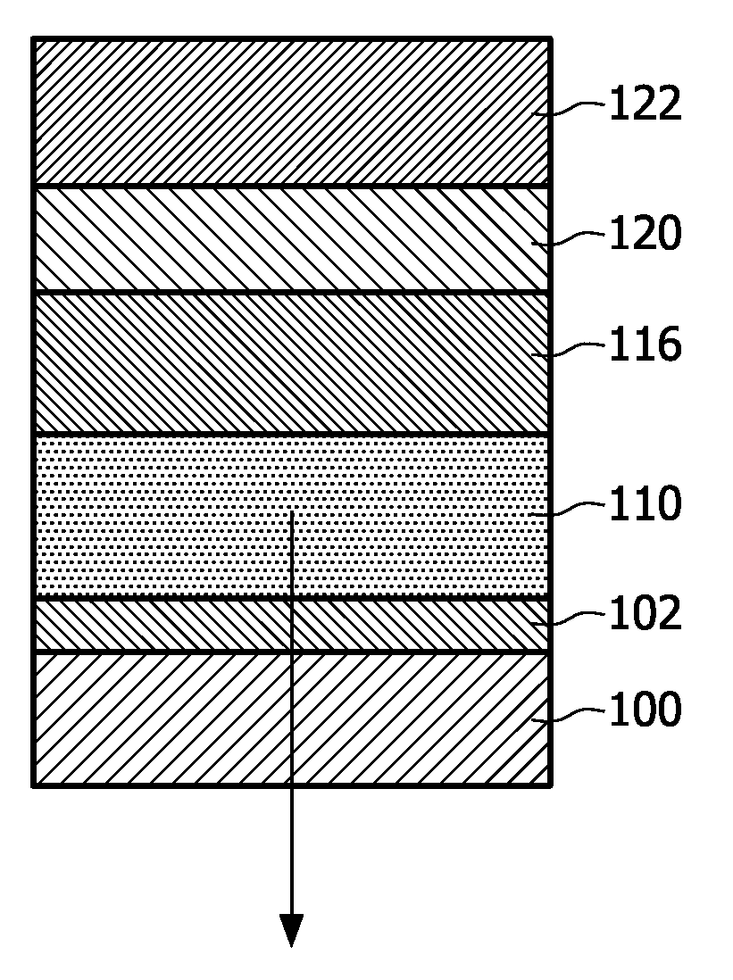
[0029]FIG. 1 schematically shows a cross-sectional view of layers in an electro-optically active organic diode according to an embodiment. The organic diode comprises a substrate 100, an anode layer 102, an electro-optically active organic layer 110, a charge carrier organic layer 116, an inorganic short protection layer 120 and a cathode layer 122.

[0030]The substrate 100 is typically transparent and may for example be made of a ceramic, e.g. glass or silicon, a plastic or a metal. The substrate may be rigid or flexible.

[0031]The anode layer 102 is a hole-injecting layer, typically of a relatively high work function and electrically conducting material, and is typically transparent in order to let light through, which is indicated by an arrow in FIG. 1. One currently predominant example of a transparent material suitable for the anode layer is indium tin oxide (ITO). Other examples include metals, metal oxides, doped inorganic semiconductors, doped conducting polymers or small molec...


PUM


Abstract

An electro-optically active organic diode has anode electrode (102), a cathode electrode (122), an electro-optically active organic layer (110) arranged between the electrodes (102, 122) and a charge carrier organic layer (116) arranged between said electro-optically active organic layer (110) and said cathode electrode layer (122), and adjacent to said electro-optically active organic layer (110). The charge carrier organic layer (116) is formed of a highly doped organic semiconductor material. A short protection layer (120) is arranged between said cathode electrode layer (122) and said charge carrier organic layer (116), and adjacent to said cathode electrode layer (122), wherein said short protection layer (120) is formed of an inorganic semiconductor material. The short protection layer prevents direct contact between the cathode layer and the charge carrier organic layer, which reduces the risk that the cathode layer will have detrimental impact on the charge carrier organic layer. This reduces the risk of a short to occur between the cathode and the anode, which results in increased reliability of the organic diode.

Description

FIELD OF THE INVENTION[0001]The present invention relates generally to electro-optically active organic diodes, such as used in organic solar cells and as organic light emitting diodes (OLEDs). More specifically it relates to an electro-optically active organic diode comprising an anode electrode, a cathode electrode, an electro-optically active organic layer arranged between the electrodes, and a charge carrier organic layer formed of a highly doped organic semiconductor material.BACKGROUND OF THE INVENTION[0002]Electro-optically active organic diodes are for example used as organic light emitting diodes (OLEDs), in lightning devices, in display devices and in organic solar cell devices. An organic diode in an organic solar cell device is arranged to generate electricity from light, whilst in a lightning device, the organic diode is arranged to generate light from electricity. Nevertheless, these are just different manifestations of common fundamental properties pertaining to certa...

Claims


Application Information

Patent Timeline
Patent Type & Authority Applications(United States)
IPC IPC(8): H01J1/63
CPCH01L51/5092H01L51/5052H10K50/155H10K50/165H10K50/171H01L27/1244H10K2102/351
Inventor BUCHEL, MICHAELBERTRAM, DIETRICH
Owner BEIJING XIAOMI MOBILE SOFTWARE CO LTD
Why Eureka
Try Eureka