Light emission device and display device using the same as light source

a technology of light emission device and light source, which is applied in the direction of instruments, discharge tubes, luminescnet screens, etc., can solve the problems of deteriorating the driving stability of the light emission device, requiring a large amount of time and cost for manufacturing the conventional electron emission unit, and the method of manufacturing the electron emission unit becomes very complicated, so as to improve the structure of the electron emission unit, improve the manufacturing process, and reduce the manufacturing cost

Inactive Publication Date: 2009-07-09
SAMSUNG SDI CO LTD
View PDF11 Cites 6 Cited by
  • Summary
  • Abstract
  • Description
  • Claims
  • Application Information

AI Technical Summary

Benefits of technology

[0011]In accordance with the present invention a light emission device is provided which simplifies its manufacturing process and lowers its manufacturing cost by improving the structure of an electron emission unit and improving driving stability by improving withstanding voltage characteristics of a cathode electrode and a gate electrode. A display device is also provided having the light emission device in accordance with the present invention as a light source.

Problems solved by technology

As described above, the method for manufacturing the electron emission unit becomes very complicated.
Therefore, a large amount of time and cost are required for manufacturing the conventional electron emission unit.
The resulting electric charge at the insulation layer lowers withstanding voltage characteristics of the cathode electrode and the gate electrode, thereby seriously deteriorating the driving stability of the light emission device.

Method used


Image

  • Light emission device and display device using the same as light source
  • Light emission device and display device using the same as light source
  • Light emission device and display device using the same as light source

Examples


Embodiment Construction

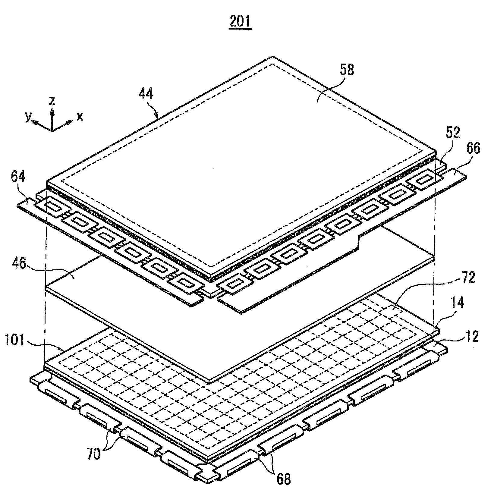
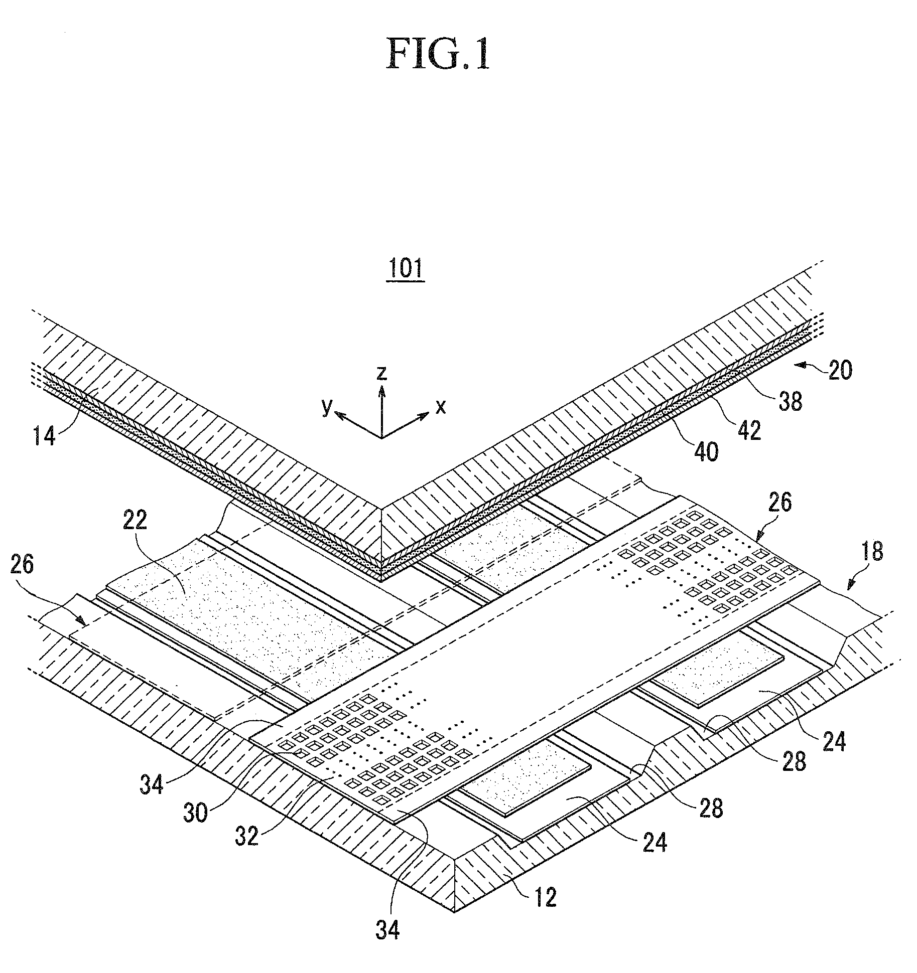
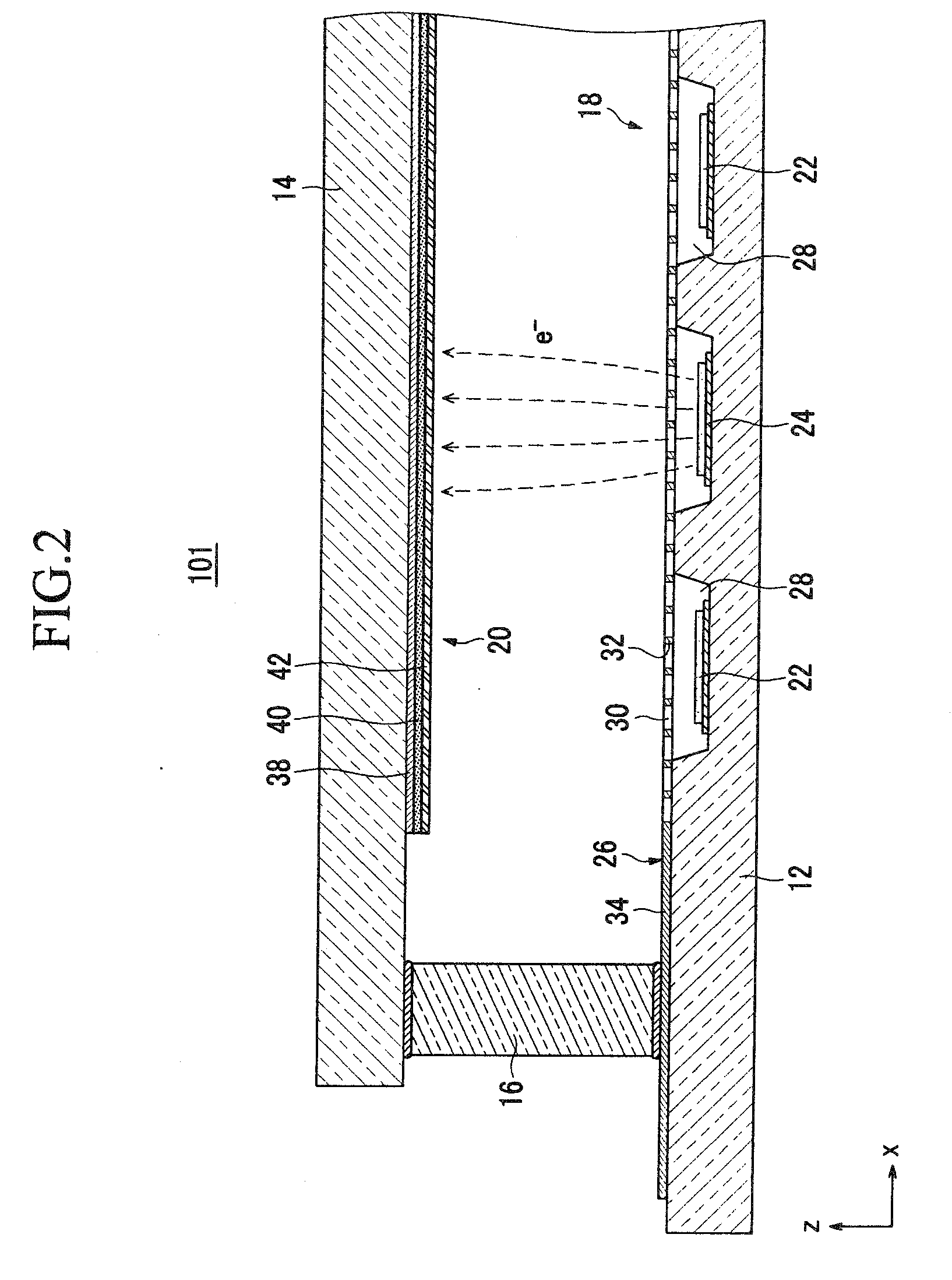
[0032]Referring to FIG. 1 and FIG. 2, the light emission device 101 according to the present exemplary embodiment includes a vacuum panel. The vacuum panel includes a first substrate 12 and a second substrate 14 facing each other, and a sealing member 16 between the first and second substrates 12, 14 for bonding the first and second substrates 12, 14 together. The inside of the vacuum panel is sustained at a vacuum degree of about 10−6 Torr.

[0033]In the first and second substrates 12, 14, a region within the sealing member 16 is divided into a light emitting region for emitting visible light and a non-light emitting region surrounding the light emitting region. An electron emission unit 18 for emitting electrons is located at the light emitting region in the first substrate 12, and a light emission unit 20 for emitting visible light is located in the light emitting region in the second substrate 14.

[0034]The second substrate 14 having the light emission unit 20 may be a front substr...


PUM

PropertyMeasurementUnit
widthaaaaaaaaaa
depthaaaaaaaaaa
thicknessaaaaaaaaaa

Abstract

A light emission device for simplifying a structure of an electron emission unit and a manufacturing process thereof is provided. A display device using the light emission device as a light source is also provided. The light emission device includes a vacuum panel having a first substrate and a second substrate facing each other. A sealing member is between the first and second substrates. Recesss portions each have a depth into a side of the first substrate facing the second substrate. Cathode electrodes are in corresponding recesses. Electron emission regions are on corresponding cathode electrodes. A gate electrode is fixed at one side of the first substrate at a distance from the electron emission regions. A light emission unit is at one side of the second substrate. The gate electrode includes a mesh unit having openings for passing through an electron beam and a supporting member surrounding the mesh unit.

Description

CROSS-REFERENCE TO RELATED APPLICATION[0001]This application claims priority to and the benefit of Korean Patent Application No. 10-2008-0002571 filed in the Korean Intellectual Property Office on Jan. 9, 2008, the entire contents of which are incorporated herein by reference.BACKGROUND OF THE INVENTION[0002]1. Field of the Invention[0003]The present invention relates to a light emission device and a display device using the light emission device as a light source. More particularly, the present invention relates to an electron emission unit in a light emission device and that emits electrons toward a phosphor layer.[0004]2. Description of the Related Art[0005]There are many different types of light emission devices that radiate visible light. Some light emission devices include an anode electrode and a phosphor layer on a front substrate and an electron emission region and driving electrodes on a rear substrate. The front and rear substrates are sealed to each other at their periph...

Claims


Application Information

Patent Timeline
Patent Type & Authority Applications(United States)
IPC IPC(8): G02F1/13357H01J63/04G09F13/08
CPCG02F1/133602H01J63/06H01J63/02G02F2001/133625G02F1/133625H01J1/30H01J31/12
Inventor JUNG, KYU-WONKIM, HUN-SOOLEE, SANG-JINKIM, IL-HWANLEE, CHANG-SOOHWANG, MYUNG-ICKSEON, HYEONG-RAE
Owner SAMSUNG SDI CO LTD
Why Eureka
Try Eureka