Method for forming a die-attach layer during semiconductor packaging processes

a technology of die-attaching layer and semiconductor packaging, which is applied in the direction of semiconductor devices, semiconductor/solid-state device details, electrical equipment, etc., can solve the problems of substrate warpage, die-attach material bleed, and difficulty in printing liquid-type die-attach materials, so as to reduce packaging costs, reduce equipment costs, and reduce material costs

Inactive Publication Date: 2009-07-09
POWERTECH TECHNOLOGY
View PDF2 Cites 3 Cited by
  • Summary
  • Abstract
  • Description
  • Claims
  • Application Information

AI Technical Summary

Benefits of technology

[0020]Therefore, by the method for forming a die-attach layer during semiconductor packaging processes revealed in the present invention, lower material costs of liquid adhesive or paste-type adhesive (die-attach materials 230) with lower equipment costs of stencil printing can be implemented to form a die-attach layer to reduce packaging costs and to increase package reliability by a die-attaching enhanced chip carrier having an exposed core for die bonding. The warpage of the chip carrier is restrained to avoid handling and alignment issues due to substrate warpage in the following packaging processes leading to higher packaging productivity and better package quality. Furthermore, the bleeding of the die-attach material 230 is eliminated to ensure good electrical contacts of the bonding wires 320 leading better package reliability.

Problems solved by technology

The former has the advantages of saving die-attach materials with flexible printing die-attaching area, however, it is very sensitive to substrate warpage leading to bleeding of die-attach materials.
Since only the bottom solder mask 112 is disposed on the bottom surface 114 of the substrate 110, substrate warpage become worse, especially using substrate strips for semiconductor packaging, leading to difficulties of printing liquid-type die-attach materials directly on the core layer 111 of the substrate 110.
Moreover, a substrate strip with severe substrate warpage can not easily be transported nor handled by the packaging equipment during packaging processes.
However, it is very difficult to print liquid-type die-attach materials on each individual substrate unit, moreover, individual substrate units are also very difficult to transport and handle by the packaging equipment during packaging processes.
Handling individual substrate units will greatly increase packaging costs.

Method used


Image

  • Method for forming a die-attach layer during semiconductor packaging processes
  • Method for forming a die-attach layer during semiconductor packaging processes
  • Method for forming a die-attach layer during semiconductor packaging processes

Examples


Embodiment Construction

[0011]Please refer to the attached drawings, the present invention will be described by means of embodiment below.

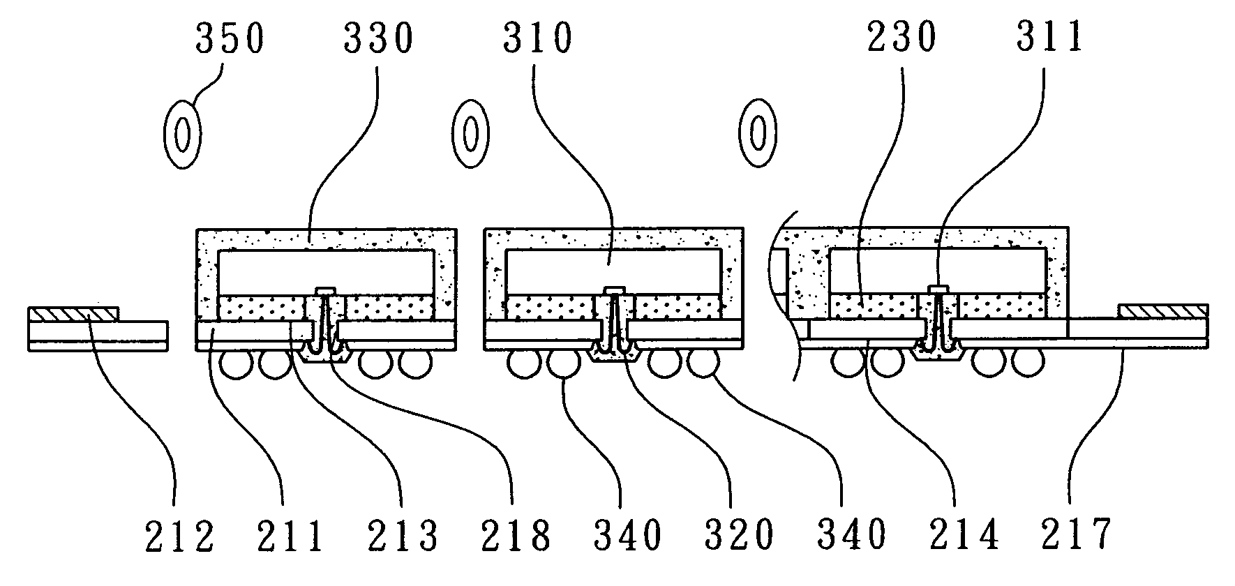
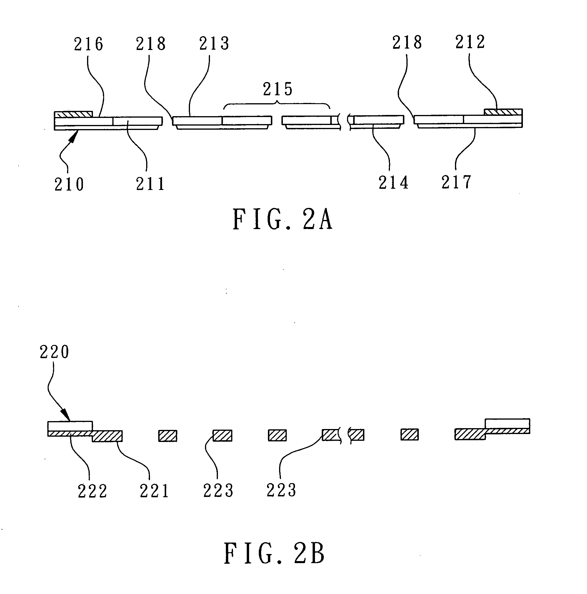
[0012]A method for forming a die-attach layer during semiconductor packaging processes is revealed as shown from FIG. 2A to 2E. Firstly, as shown in FIG. 2A and FIG. 3, a chip carrier 210 is provided where the chip carrier 210 includes a substrate core 211 and a stiffener 212. The top surface 213 of the substrate core 211 includes a plurality of die-attaching units 215 and a peripheral area 216 enclosing the die-attaching units 215. As shown in FIG. 3, the stiffener 212 is attached to some portion of the top surface 213 of the substrate core 211 to cover the peripheral area 216 without covering the die-attaching units 215 to enhance the strength of the chip carrier 210 and to avoid warpage of the chip carrier 210 for the following semiconductor packaging processes. In the present embodiment, the chip carrier 210 can be a printed circuit board having a bottom solder mask ...


PUM


Abstract

Disclosed is a method for forming a die-attach layer during semiconductor packaging processes. A chip carrier includes a substrate core and a stiffener. Top surface of the substrate core includes a plurality of die-attaching units and a peripheral area enclosed by the stiffener. A non-planar printing stencil is also provided. When the non-planar printing stencil is pressed against the chip carrier, the non-planar printing stencil is compliantly in contact with the substrate core and the stiffener and a plurality of printing openings of the non-planar printing stencil exposes the substrate core within the die-attaching units. During stencil printing, die-attach material fills in the printing openings to directly adhere to the substrate core. Therefore, the warpage of the substrate core is restrained to avoid bleeding of die-attach material so that die-attach materials can be formed as a die-attach layer with a uniform thickness on core-exposed chip carrier with lower costs. Additionally, the chip carrier will not be deformed during semiconductor packaging processes.

Description

FIELD OF THE INVENTION[0001]The present invention relates to a fabrication technology of semiconductor devices, especially to a method for forming a die-attach layer during semiconductor packaging processes.BACKGROUND OF THE INVENTION[0002]In conventional semiconductor devices, a chip in package is attached to a substrate by a die-attach material. There are two major types of forming die-attach materials where one is in either paste or liquid disposed by printing or dispensing. Another one is utilizing a die-attach tape where the die-attach tape is preformed as a tape in solid state and then attached to a substrate. The former has the advantages of saving die-attach materials with flexible printing die-attaching area, however, it is very sensitive to substrate warpage leading to bleeding of die-attach materials. Since solder masks are disposed on both top and bottom surfaces of the substrate, therefore, the substrate warpage is not an issue for now. But when the substrate structure ...

Claims


Application Information

Patent Timeline
Patent Type & Authority Applications(United States)
IPC IPC(8): H01L21/00
CPCH01L21/481H01L24/48H01L21/561H01L23/13H01L23/3128H01L23/49833H01L24/27H01L24/83H01L24/97H01L2224/48091H01L2224/4824H01L2224/73215H01L2224/8385H01L2224/92147H01L2224/97H01L2924/01005H01L2924/01082H01L2924/07802H01L2924/15311H01L21/4867H01L2924/0665H01L2924/014H01L2924/01033H01L2224/2919H01L2224/85H01L2924/00014H01L2224/83H01L2924/00H01L2924/181H01L2224/32225H01L2924/00012H01L2224/45099H01L2224/45015H01L2924/207
Inventor FAN, WEN-JENG
Owner POWERTECH TECHNOLOGY
Why Eureka
Try Eureka