
Flash memory device including a dummy cell

a flash memory and dummy cell technology, applied in static storage, digital storage, instruments, etc., can solve the problems of reducing the cost of ssd, increasing the capacity, and affecting the programability of cell transistors, so as to increase the channel total capacitance, increase the probability of cell transistor mc30> being programmed, and increase the channel capacitance of unselected cell transistors.

Active Publication Date: 2009-07-16
SAMSUNG ELECTRONICS CO LTD
View PDF8 Cites 32 Cited by
  • Summary
  • Abstract
  • Description
  • Claims
  • Application Information

AI Technical Summary

Benefits of technology

[0003]Generally, NAND flash memory devices are programmed and erased using Fowler-Nordheim (F-N) tunneling. In F-N tunneling, electrons are injected / discharged from / to a channel region into / from a floating gate due to a large voltage difference between the channel region and a control gate of a cell transistor. Because of the relative ease in programming and erasing NAND flash memory devices, NAND flash memory devices are known to have good data storage characteristics as compared to other non-volatile memory devices. Moreover, NAND flash memory devices are also capable of high density integration, low power dissipation, and durability of percussion. These and other such features have helped increase the usage of NAND flash memory devices in recent years.
[0004]For example, the NAND flash memory is increasingly considered as a substitute for hard disk driver (HDD) as an auxiliary memory unit that is known as a solid state disk (SSD). While a SSD is considered to be inferior in capacity and cost to the HDD, the SSD is considered to be superior in access speed, miniaturization, and durability of percussion to the HDD. Moreover, it is expected that the progress of design and process technologies may increase the capacity and decrease the cost of the SSD. For these reasons, the SDD may be increasingly used as an auxiliary memory unit instead of the HDD.
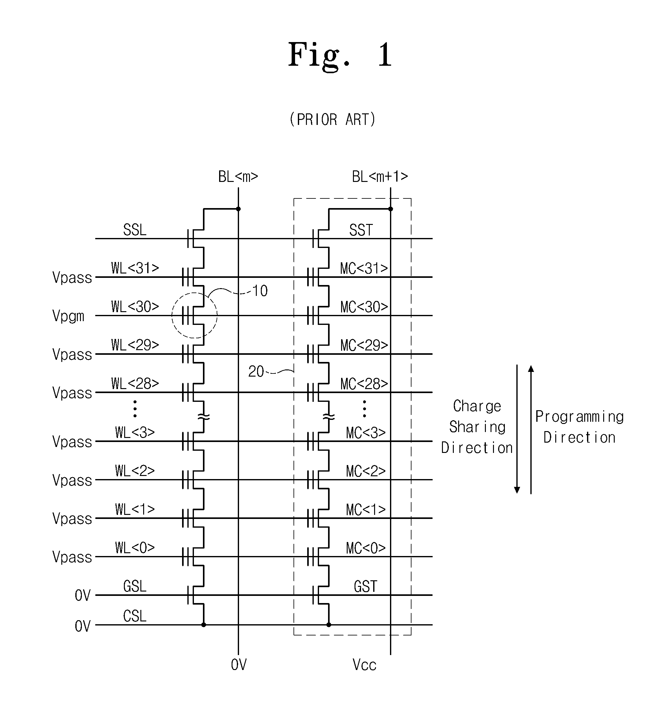
[0010]A local self-boosting scheme may be used to solve the above-mentioned problem. As depicted in FIG. 1, arrows indicate a charge-sharing direction and a programming direction. According to the local self-boosting scheme, a ground voltage of 0V is applied to two unselected word lines disposed at both sides of a selected word line. Furthermore, a program voltage Vpgm is applied to the selected word line after the pass voltage Vpass (e.g., about 10V) is applied to the remaining unselected word lines. Under the bias condition, the channel of a program-inhibited memory cell is locally boosted and the inactivated channels of two memory cells adjacent to the program-inhibited memory cell enables charges in the locally boosted channel to be blocked. As a result, the channel voltage of the program-inhibited memory cell is preserved so that the F-N tunneling in the program-inhibited memory cell is prevented.
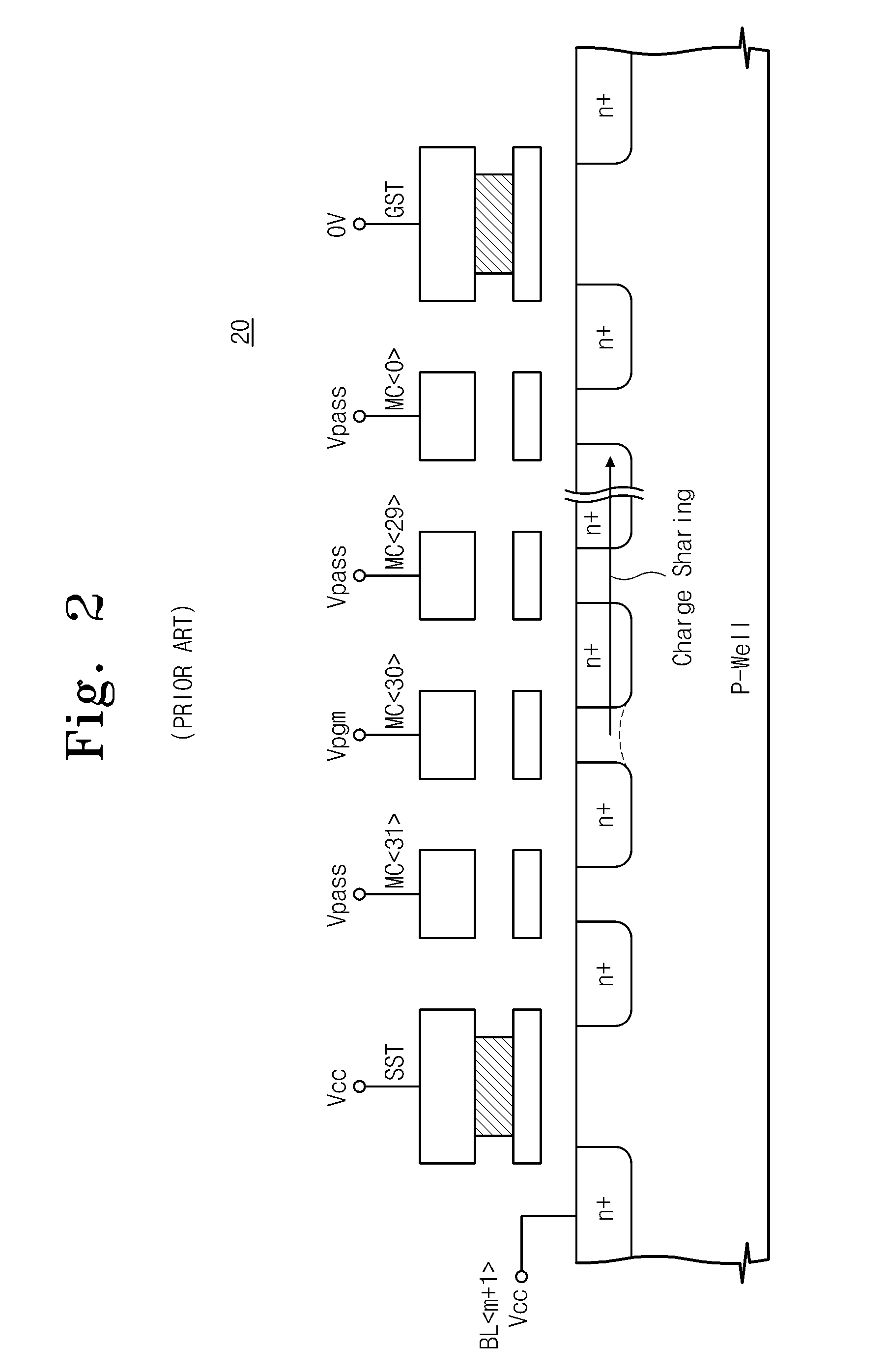
[0013]The above-mentioned drawback may become an important issue in a NAND flash memory device which starts a programming operation from a word line WL<0> in an ascending order. In other words, in a case where a selected word line is closer to the string selection transistor SST, the number of cell transistors which cause the charge sharing increase. This means that the total capacitance of channels increases as a selected word line becomes closer to the string selection transistor SST. Accordingly, as the channel capacitance of the unselected cell transistors increases, the charge shared amongst the cell transistor MC<30> and the unselected cell transistors increases, thus increasing the likelihood that the cell transistor MC<30> is programmed.

Problems solved by technology

While a SSD is considered to be inferior in capacity and cost to the HDD, the SSD is considered to be superior in access speed, miniaturization, and durability of percussion to the HDD.
Moreover, it is expected that the progress of design and process technologies may increase the capacity and decrease the cost of the SSD.
While an increase in the integration density of memory cells in a semiconductor device may help reduce the size of the device, an increase in integration density may also cause problems.
This programming of program-inhibit cells is generally undesirable.
While the above-mentioned self-boosting scheme may be used to program-inhibit a memory cell, this scheme may not work as well in a high integration density memory device.
This increase in the potential difference between the gate and channel may lead to an undesirable programming operation.
Thus, because of the relatively large coupling ratio between unselected world lines and a selected word line, it may be undesirable to apply the local self boosting scheme to a highly integrated flash memory.
This drop in the channel voltage of the cell transistor MC30> may lead to an undesirable programming operation due to increase in a voltage difference between the gate and the channel.
The above-mentioned drawback may become an important issue in a NAND flash memory device which starts a programming operation from a word line WL0> in an ascending order.

Method used


Image

  • Flash memory device including a dummy cell
  • Flash memory device including a dummy cell
  • Flash memory device including a dummy cell

Examples


Embodiment Construction

[0040]The present invention will now be described more fully hereinafter with reference to the accompanying drawings, in which preferred embodiments of the invention are shown. This invention, however, may be embodied in many different forms and should not be construed as limited to the embodiments set forth herein. Rather, these embodiments are provided so that this disclosure will be thorough and complete, and will fully convey the scope of the invention to those skilled in the art.

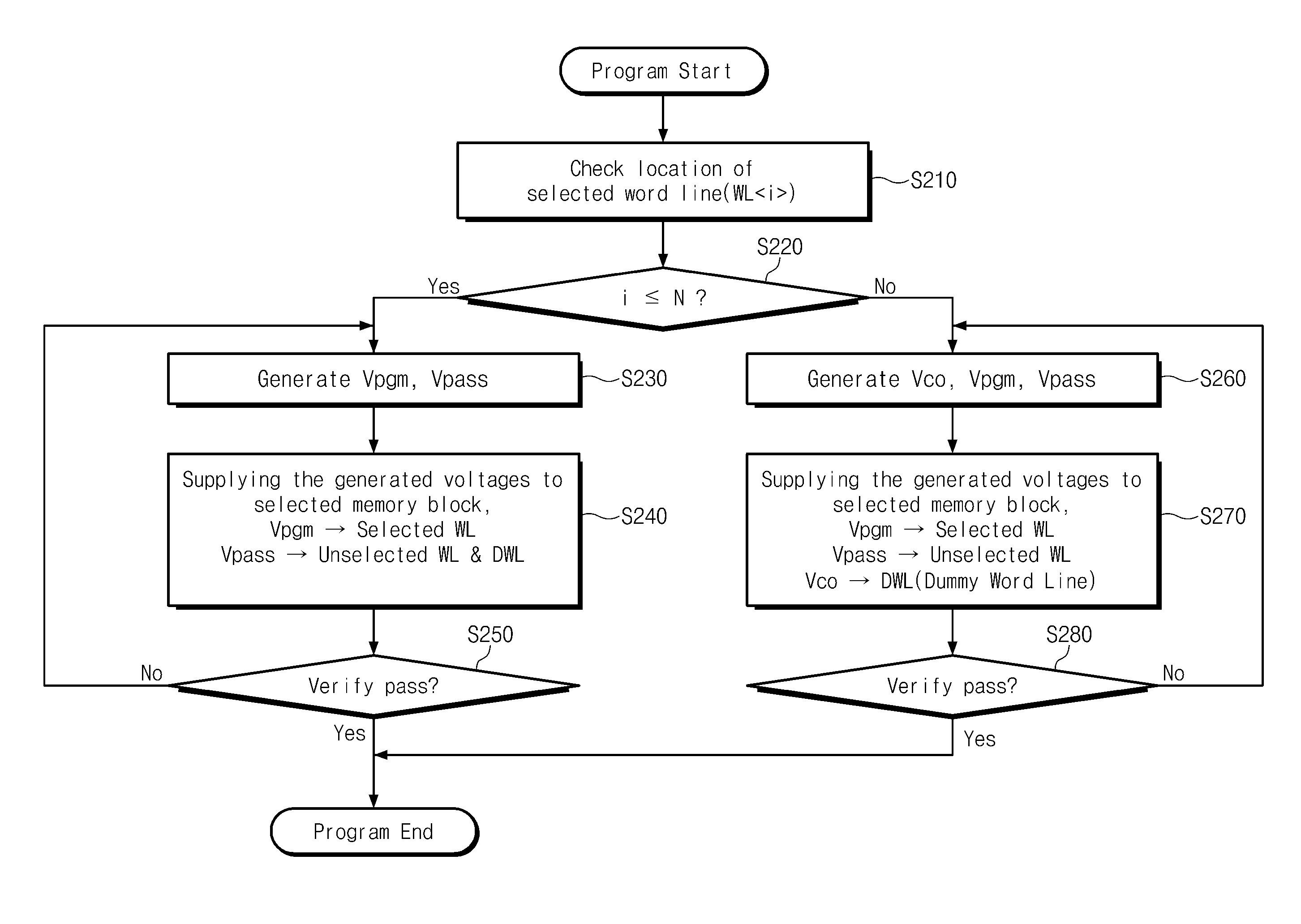
[0041]FIG. 4 shows a schematic circuit diagram of an array structure according to an exemplary embodiment. Referring to FIG. 4, a dummy cell DMC is placed in each of strings 30. In each string 30, the dummy cell DMC blocks the sharing of charges being boosted in a channel of a program-inhibited cell. Furthermore, in each of the strings 30, the dummy cell DMC has the same characteristics and performance as other memory cells in a corresponding sting. Generally, each of the strings includes 32 memory cell...


PUM


Abstract

A non-volatile memory device includes a selection transistor coupled to a bit line. The device also includes a plurality of memory cells serially coupled to the selection transistor and at least one dummy cell located between the plurality of memory cells. The dummy cell is turned off during a programming operation of a memory cell located between the dummy cell and the selection transistor.

Description

CROSS-REFERENCE TO RELATED APPLICATIONS[0001]This is a continuation-in-part of U.S. non-provisional patent application Ser. No. 11 / 523,571, filed Sep. 20, 2006, the disclosure of which is incorporated herein by reference in its entirety. In addition, a claim of priority 35 U.S.C § 119 is made to Korean Patent Application Nos. 2006-0002310 and 2008-0036195, filed Jan. 9, 2006, and Apr. 18, 2008, respectively, the disclosures of which are incorporated herein by reference in their entirety.SUMMARY[0002]The present invention generally relates to semiconductor memory devices, and more particularly, the present invention relates to NAND flash memory devices.[0003]Generally, NAND flash memory devices are programmed and erased using Fowler-Nordheim (F-N) tunneling. In F-N tunneling, electrons are injected / discharged from / to a channel region into / from a floating gate due to a large voltage difference between the channel region and a control gate of a cell transistor. Because of the relative ...

Claims


Application Information

Patent Timeline
IPC IPC(8): G11C16/06
CPCG11C16/0483G11C11/5628
Inventor KANG, HEE-SOOCHOI, DONG-UKLEE, CHOONG-HOKANG, SANG-GU
Owner SAMSUNG ELECTRONICS CO LTD
Learn More