
Manufacturing method and manufacturing apparatus of semiconductor substrate

Inactive Publication Date: 2009-07-16
SEMICON ENERGY LAB CO LTD
View PDF5 Cites 18 Cited by
  • Summary
  • Abstract
  • Description
  • Claims
  • Application Information

AI Technical Summary

Benefits of technology

[0011]In view of the above-described problems, it is an object of the present invention to provide a homogeneous semiconductor substrate in which defective bonding is reduced. It is another object of the present invention to manufacture the semiconductor substrate with high yield and provide a manufacturing apparatus of the semiconductor substrate, which is suitable for the manufacturing method.
[0020]As described above, in the present invention, bonding is performed by applying pressure to one of the corner portions of the substrate. As a result of this, possibility of generation of defective bonding due to trapping of air, a mismatch of the interface, or the like can be reduced. Further, after the bonding and before transfer of the substrates, heat treatment is performed in order to strengthen the bonding of the substrates. As a result of this, separation of the substrates due to bending of the base substrate in transfer can be prevented. That is, by the manufacturing method and the manufacturing apparatus of the present invention, defective bonding can be reduced, so that a semiconductor substrate can be manufactured with high yield.

Problems solved by technology

For example, when the bonding is performed by applying even pressure to the entire surfaces of the substrates, since the bonding progresses from a plurality of regions at the same time, defective bonding due to trapping of air or a mismatch of the interface, or the like is likely to be generated.
Further, separation of the substrates after the bonding is also a serious problem.
These problems become more serious in the case of manufacturing a semiconductor substrate having a large area in which a plurality of silicon substrates is bonded to one base substrate.

Method used


Image

  • Manufacturing method and manufacturing apparatus of semiconductor substrate
  • Manufacturing method and manufacturing apparatus of semiconductor substrate
  • Manufacturing method and manufacturing apparatus of semiconductor substrate

Examples


embodiment mode 1

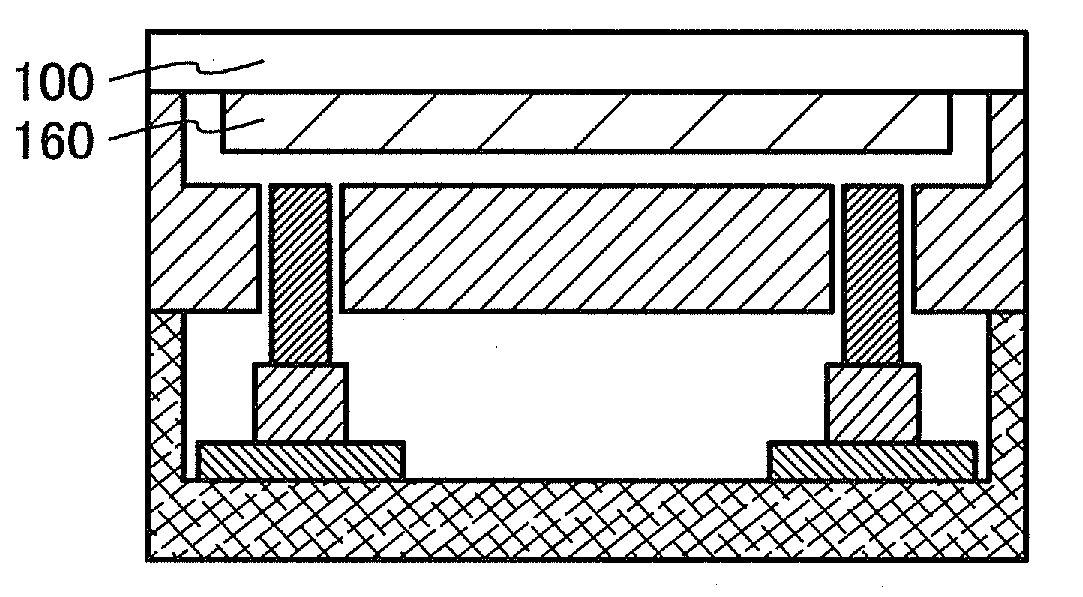
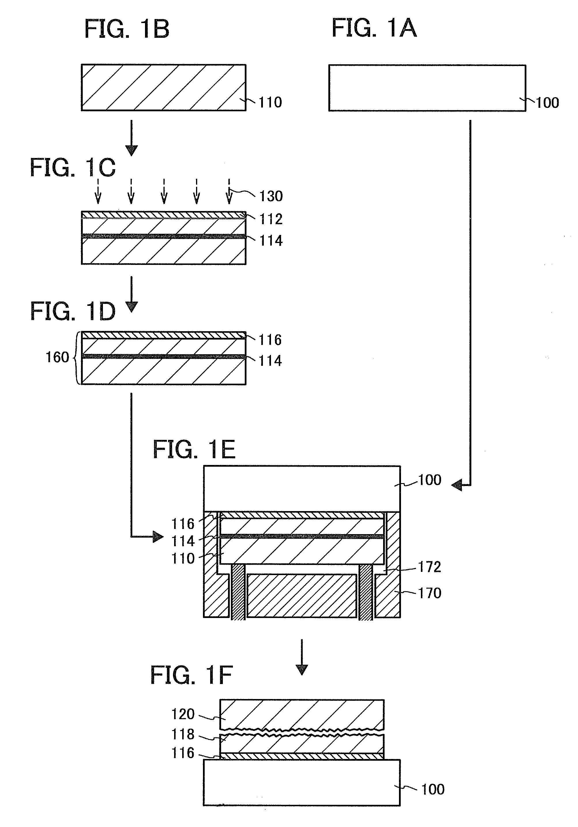
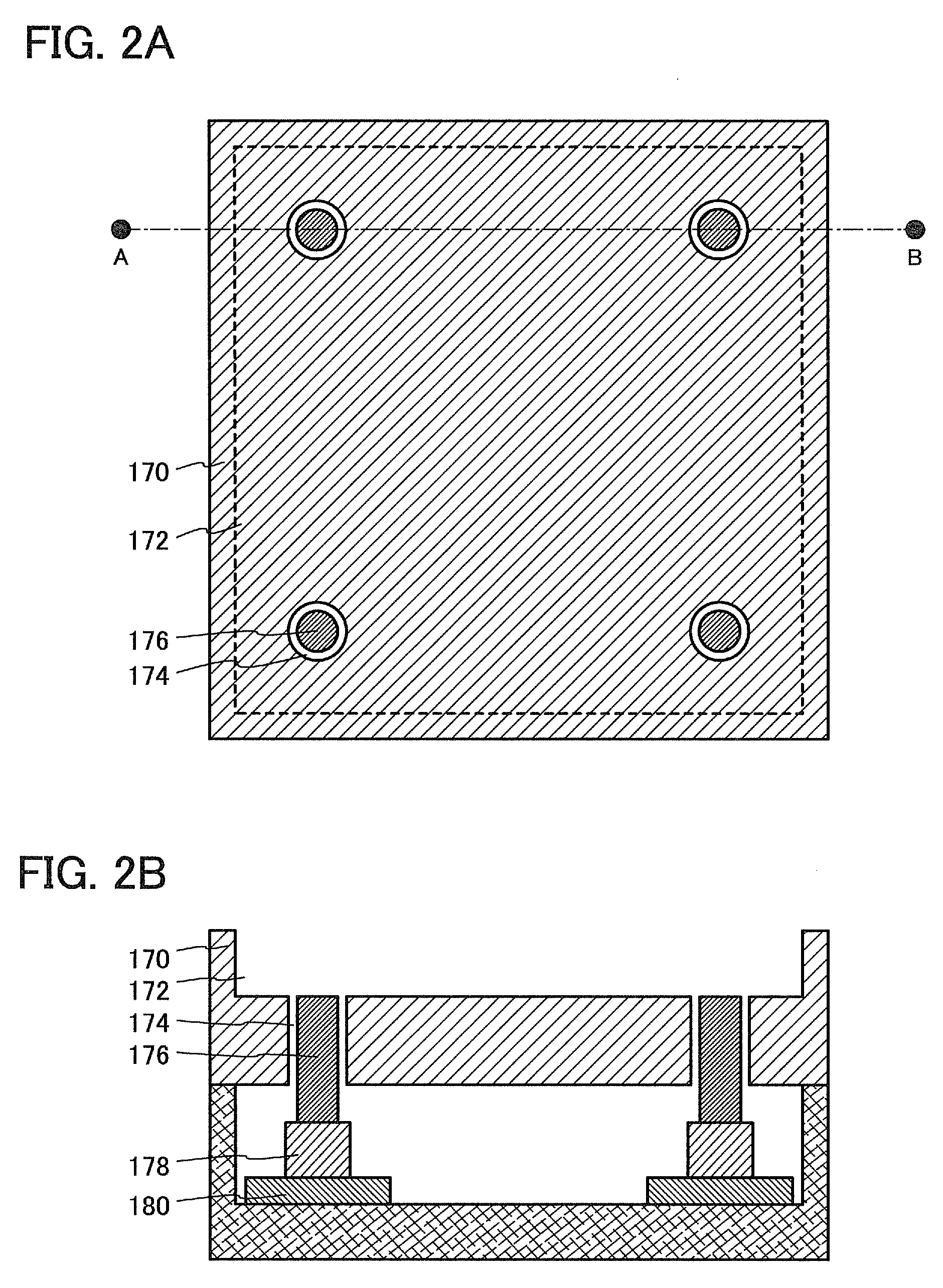
[0048]In this embodiment mode, an example of a manufacturing method of a semiconductor substrate of the present invention will be described with reference to FIGS. 1A to 1F, FIGS. 2A and 2B, FIGS. 3A to 3D, and FIGS. 4A to 4C.

[0049]First, a base substrate 100 is prepared (see FIG. 1A). As the base substrate 100, a light-transmitting glass substrate used for a liquid crystal display device or the like can be used. A substrate having a strain point of greater than or equal to 580° C. (preferably greater than or equal to 600° C.) may be preferably used as a glass substrate. Further, it is preferable that the glass substrate be a non-alkali glass substrate. As a material for the non-alkali glass substrate, a glass material such as aluminosilicate glass, aluminoborosilicate glass, or barium borosilicate glass is used, for example.

[0050]Note that, as the base substrate 100, in addition to the glass substrate, an insulating substrate which is formed of an insulating material, such as a cer...

embodiment mode 2

[0102]In this embodiment mode, a manufacturing method of a semiconductor substrate having a plurality of single crystal semiconductor layers will be described with reference to FIGS. 5A and 5B and FIGS. 6A to 6D. Note that there are many common points between the manufacturing method of a semiconductor substrate of this embodiment mode and the manufacturing method of a semiconductor substrate of Embodiment Mode 1. Therefore, in this embodiment mode, different points will be mainly described and the descriptions of the common points are partially omitted.

[0103]First, by the method described in Embodiment Mode 1, the base substrate 100 and the single crystal semiconductor substrate 110 are processed (see FIGS. 1A to 1D). Note that in this embodiment mode, a case will be described in which a plurality of single crystal semiconductor layers is provided over the base substrate 100. That is, it needs to be noted that since a plurality of single crystal semiconductor substrates 110 is used...

embodiment mode 3

[0124]In this embodiment mode, another example of a manufacturing method of a semiconductor substrate having a single crystal semiconductor layer will be described with reference to FIGS. 7A to 7C. Note that in this embodiment mode, a state of bonding and an apparatus for bonding will be briefly described.

[0125]FIG. 7A illustrates an example of a state of bonding and an apparatus for bonding in this embodiment mode. Here, the substrate 160 is disposed in a substrate arrangement region 772 of a substrate supporting base 770 and the base substrate 100 is fixed with the use of a mechanism 700 having substrate supporting mechanisms 776 and raising and lowering mechanisms 778. Here, the substrate supporting mechanism 776 includes a mechanism which adsorbs the base substrate 100. That is, in FIG. 7A, the base substrate 100 is not in contact with the substrate supporting base 770. In bonding, the base substrate 100 is lowered by the substrate supporting mechanisms 776 and the raising and l...


PUM

PropertyMeasurementUnit
Temperatureaaaaaaaaaa
Pressureaaaaaaaaaa

Abstract

It is an object to provide a homogeneous semiconductor substrate in which defective bonding is reduced. Such a semiconductor substrate can be formed by the steps of: disposing a first substrate in a substrate bonding chamber which includes a substrate supporting base where a plurality of openings is provided, substrate supporting mechanisms provided in the plurality of openings, and raising and lowering mechanisms which raise and lower the substrate supporting mechanisms; disposing a second substrate over the first substrate so as not to be in contact with the first substrate; and bonding the first substrate to the second substrate by using the raising and lowering mechanisms to raise the substrate supporting mechanisms.

Description

BACKGROUND OF THE INVENTION[0001]1. Field of the Invention[0002]The present invention relates to a manufacturing method and a manufacturing apparatus of a semiconductor substrate.[0003]2. Description of the Related Art[0004]In recent years, integrated circuits using an SOI (silicon on insulator) substrate, instead of using a bulk silicon substrate, have been developed. By utilizing characteristics of a thin single crystal silicon layer formed over an insulating layer, transistors formed in the integrated circuit can be electrically separated from each other completely. Further, each transistor can be formed as a fully-depleted transistor, and thus a semiconductor integrated circuit with high added value such as high integration, high speed driving, and low power consumption can be realized.[0005]As a method for manufacturing an SOI substrate, a hydrogen-ion-implantation separation method in which hydrogen ion implantation and separation are combined is known. A typical process of a ...

Claims


Application Information

Patent Timeline
IPC IPC(8): H01L21/02B32B38/18B32B37/00B32B38/16B32B38/00
CPCH01L21/187Y10T156/17H01L21/76254
Inventor OMATA, TAKATSUGUMORIWAKA, TOMOAKIOHNUMA, HIDETO
Owner SEMICON ENERGY LAB CO LTD
Learn More