Package structure

a packaging structure and packaging technology, applied in the field of packaging structure, can solve the problems of poor shielding capacity or short circuit, instability of shielding caps, and increasing complexity of packaging structure, and achieve the effect of stable alignment and good shielding

Inactive Publication Date: 2009-07-23
ADVANCED SEMICON ENG INC
View PDF7 Cites 10 Cited by
  • Summary
  • Abstract
  • Description
  • Claims
  • Application Information

AI Technical Summary

Benefits of technology

[0007]The invention is directed to a package structure using the design of a substrate and a shielding cap for stably alignment the shielding cap on the substrate and providing good shielding.

Problems solved by technology

As semiconductor packaging technology develops, the package structure becomes more and more complicated.
However, during the reflow process, the shielding cap moves easily due to convection of hot air, which may cause instability of the shielding cap, poor shielding capacity or short circuit.

Method used


Image

  • Package structure
  • Package structure
  • Package structure

Examples


first embodiment

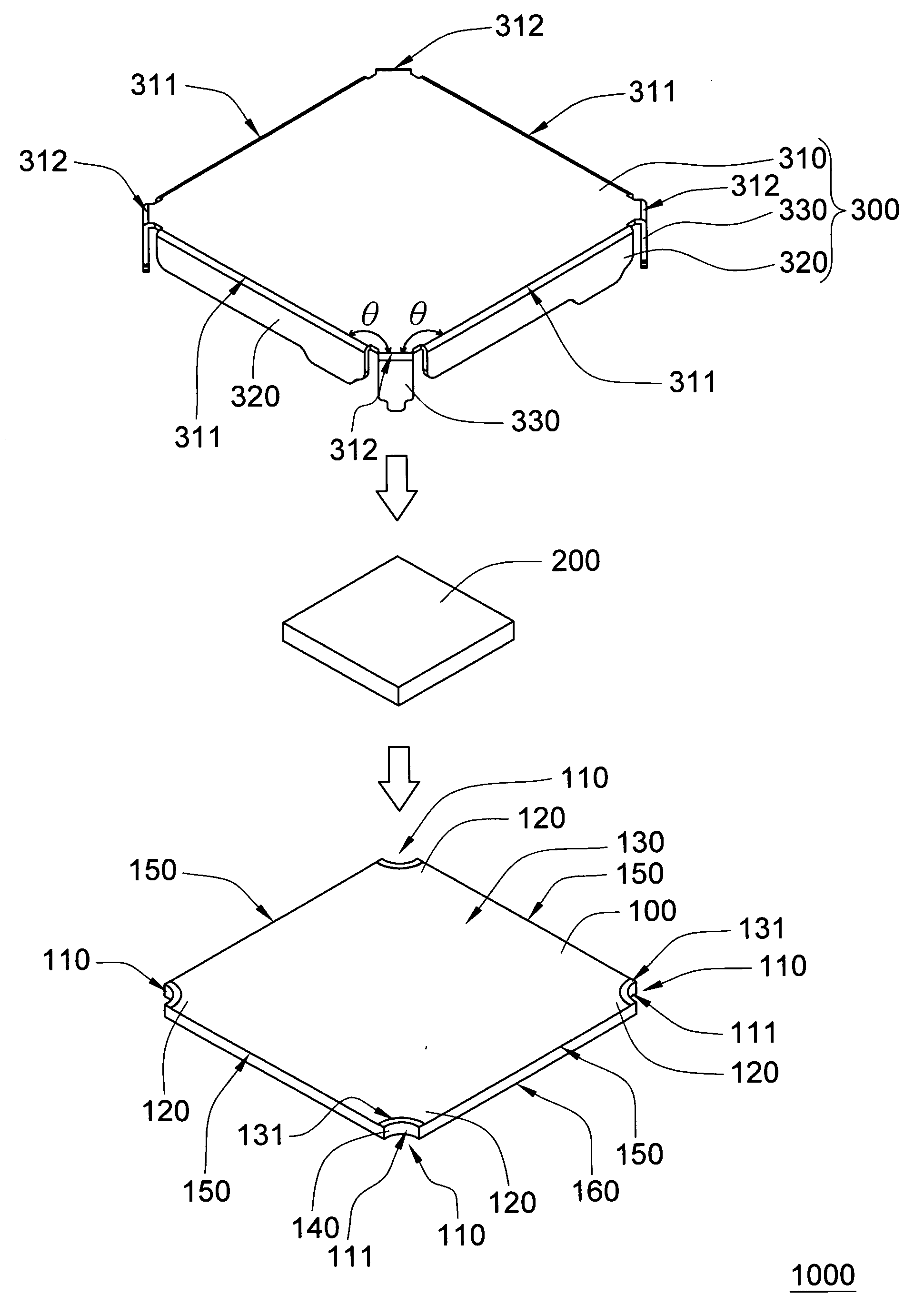
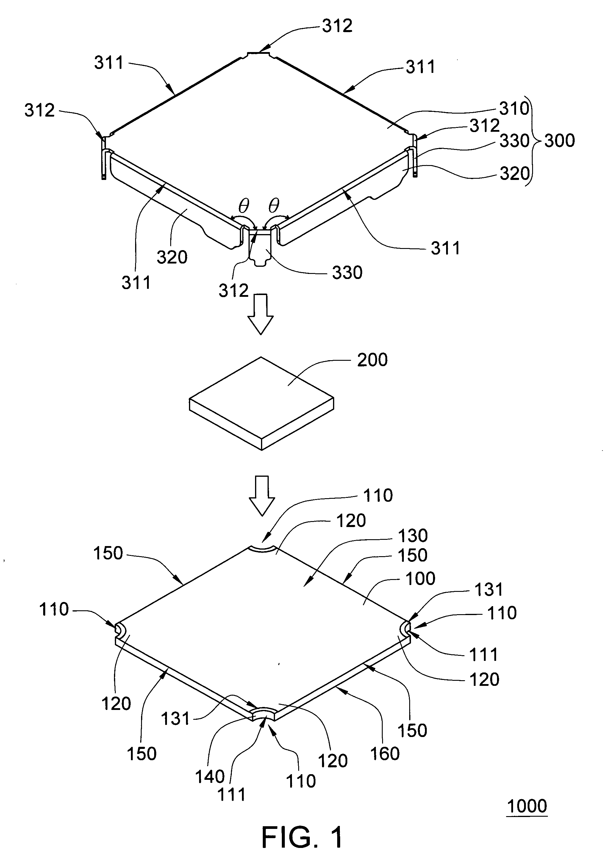
[0017]Please refer to FIG. 1. FIG. 1 is an exploded view of a package structure 1000 according to a first embodiment of the present invention. The package structure 1000 includes a substrate 100, a semiconductor device 200 and a shielding cap 300. The substrate 100 is for example a printed circuit board or a lead frame. The substrate 100 has at least an alignment recess 110. The alignment recess 110 is formed at a corner 120 of the substrate 100. In the present embodiment, the substrate 100 is substantially a quadrilateral structure. Therefore, the substrate 100 has four corners 120, and four alignment recesses 110 are respectively formed at four corners 120 of the substrate 100.

[0018]The semiconductor device 200 is for example a communication chip or a processing chip. The semiconductor device 200 is disposed on an upper surface 130 of the substrate 100. The semiconductor device 200 is for example disposed on the substrate 100 through wire-bonding or flip chip bonding.

[0019]The shi...

second embodiment

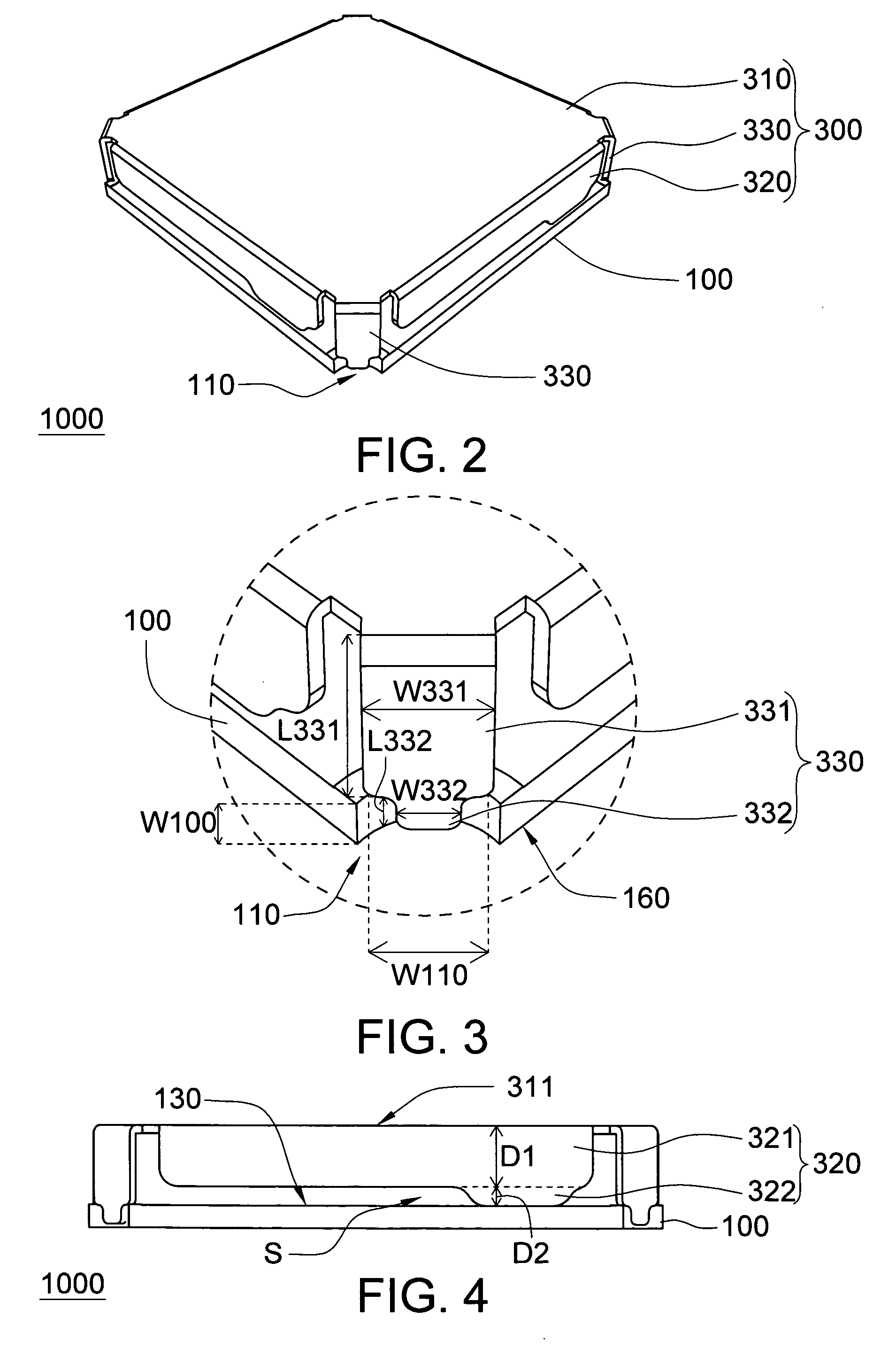
[0032]Please refer to FIG. 7. FIG. 7 illustrates the alignment pin 430 and the alignment recess 110 of the package structure 2000 according to a second embodiment of the present invention. The difference between the package structure 2000 of the present embodiment and the package structure 1000 of the first embodiment is that the alignment pin 430 of the present embodiment further includes a protruding part 433. Other parts are the same and not described repeatedly. The protruding part 433 is formed between the first pin part 331 and the second pin part 332 and leans against the inner wall 111 of the alignment recess 110. Because the protruding part 433 is formed between the first pin part 331 and the second pin part 332, the protruding part 433 leans right against the inner wall 111 on the top end of the alignment recess 110. When the solder paste is applied to part of the upper surface 131 adjacent to the alignment recess 110 and the alignment pin 430 is inserted into the alignmen...


PUM


Abstract

A package structure is provided. The package structure includes a substrate, a semiconductor device, and a shielding cap. The substrate has at least an alignment recess located at a corner of the substrate. The semiconductor device is disposed on an upper surface of the substrate. The shielding cap having an alignment pin covers the semiconductor device. The alignment pin is inserted into the alignment recess.

Description

[0001]This application claims the benefit of Taiwan application Serial No. 097102568, filed Jan. 23, 2008, the subject matter of which is incorporated herein by reference.BACKGROUND OF THE INVENTION[0002]1. Field of the Invention[0003]The invention relates in general to a package structure, and more particularly to a package structure having a shielding cap.[0004]2. Description of the Related Art[0005]As semiconductor packaging technology develops, the package structure becomes more and more complicated. For example, some processing chips and communication chips need shielding caps to protect the chips from being interfered with outer radiation, or to prevent the radiation generated by the chips from affecting other electronic units.[0006]However, during the reflow process, the shielding cap moves easily due to convection of hot air, which may cause instability of the shielding cap, poor shielding capacity or short circuit.SUMMARY OF THE INVENTION[0007]The invention is directed to a...

Claims


Application Information

Patent Timeline
Patent Type & Authority Applications(United States)
IPC IPC(8): H01L23/552
CPCH01L23/552H05K9/0026H05K9/0028H01L2924/0002H01L2924/00
Inventor LU, HSIN-CHIEH
Owner ADVANCED SEMICON ENG INC
Why Eureka
Try Eureka