Display device

a technology of a display device and a display plate, which is applied in the direction of electric apparatus casings/cabinets/drawers, instruments, planar/plate-like light guides, etc., can solve the problems of frequent breakage of glass substrates, damage to liquid crystal panels, and liable peeling, so as to improve the adhesive strength

Active Publication Date: 2009-07-23
DAWNCREST IP LLC
View PDF1 Cites 127 Cited by
  • Summary
  • Abstract
  • Description
  • Claims
  • Application Information

AI Technical Summary

Benefits of technology

[0017]Under the above-mentioned circumstances, it is an object of the present invention to provide a thin display device that is high in impact resistance without any deterioration of luminance efficiency, and does not allow a seal of a panel to be peeled off, and an electronic device that uses the display device by incorporating in a thin narrow frame shape.
[0019]That is, the display device according to the present invention includes: the display panel; the transparent member that is bonded to the display surface of the display panel with a first adhesive material; and the plate-like member that is disposed on the rear surface side of the display panel and holds the display panel, in which the transparent member and the plate-like member are bonded and fixed to each other at a portion where the transparent member and the plate-like member are overlapped with each other outside of the display panel with a second adhesive material. As a result, the impact resistance is improved.
[0020]Further, the display panel is bonded to an entire surface of the transparent member with an aid of a transparent optical adhesive layer (for example, transparent optical adhesive or transparent optical adhesive sheet) as the first adhesive material. As a result, the strength is further improved.
[0023]Further, a convex portion is formed on an outer periphery of at least a part of the plate-like member in the vicinity of an outside of the display panel, and the rear surface of the transparent member and the convex portion of the plate-like member are bonded and fixed to each other by means of the second adhesive material, to thereby further improve the adhesive strength.

Problems solved by technology

However, because those members are thinned, the glass substrate is frequently broken due to an impact caused by dropping or the like.
However, there are many cases in which a case of the main body of a cellular phone and the like is largely deformed due to the impact caused by dropping or the like, and the liquid crystal panel is damaged due to the deformation.
Further, in the structure where the liquid crystal panel and the light guide plate of the backlight are bonded tightly to each other with an aid of the elastic member, there arises such problems that peeling is liable to occur due to thermal expansion at high temperature or at low temperature, and the luminance is deteriorated because the optical sheet such as the lens sheet cannot be provided.
Because the refractive index of the optical sheet is close to the refractive index of the optical adhesive, the optical function of the optical sheet is deteriorated, and the luminance of the display surface is deteriorated.
Even in a structure where the rear surface of the liquid crystal panel is bonded to the entire surface of the light guide plate without the optical sheet, the luminance is deteriorated as compared with the backlight using the optical sheet.
In any cases described above, the optical disadvantage occurs.
In this case, the electronic device is limited in terms of design.
This leads to such a problem that the frame becomes larger.

Method used


Image

  • Display device
  • Display device
  • Display device

Examples


first embodiment

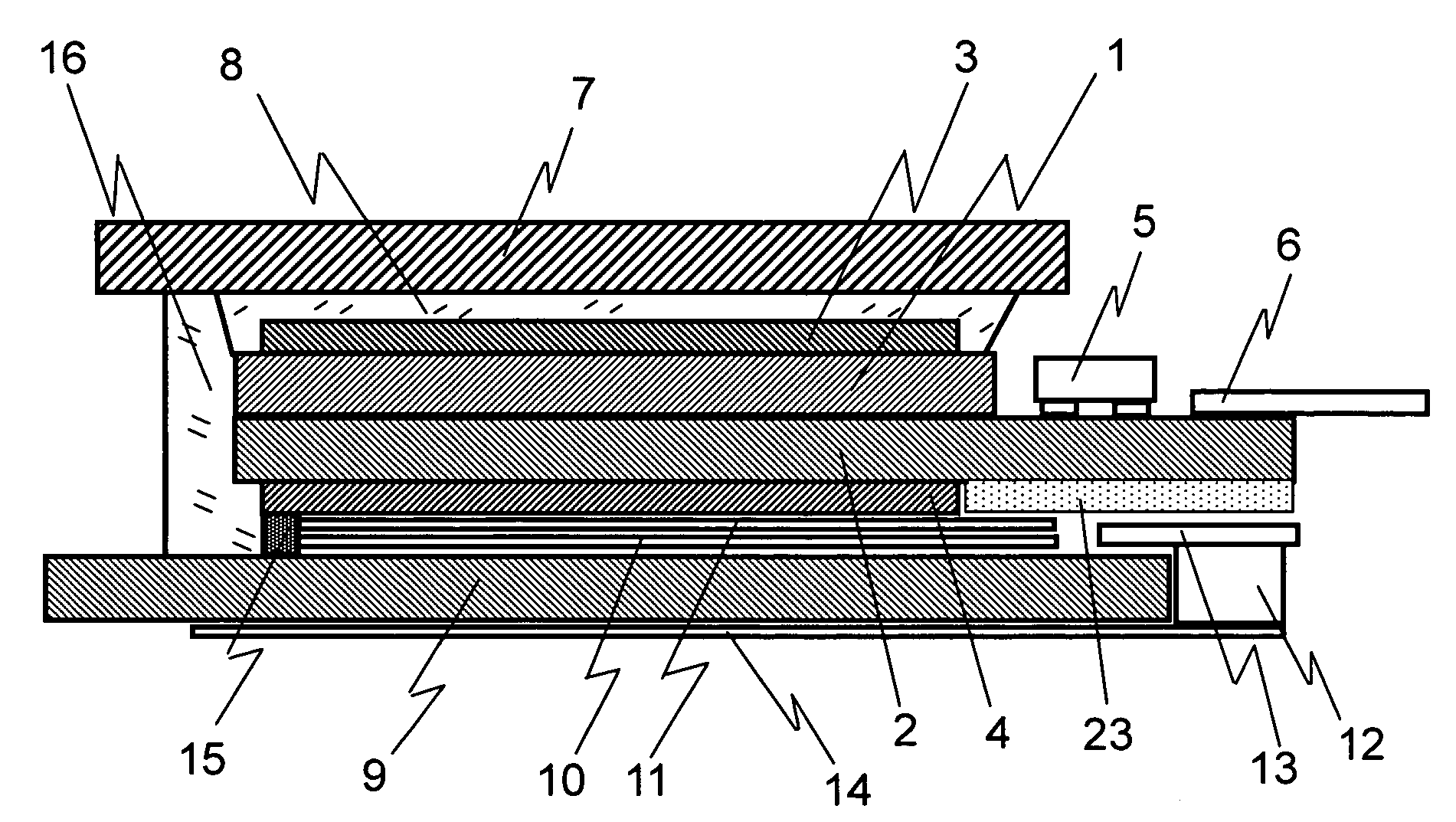
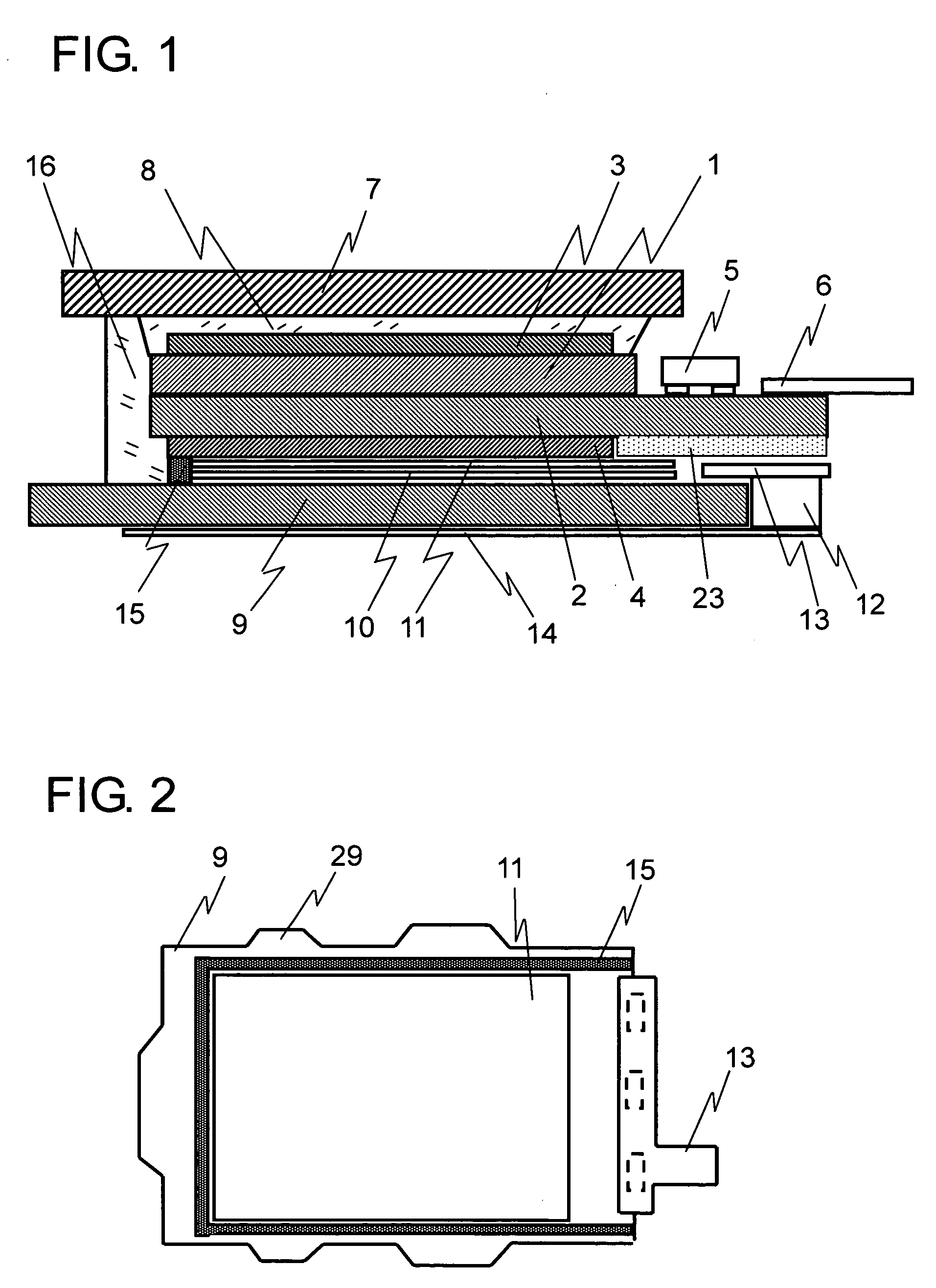
[0041]A first embodiment of the present invention is described with reference to FIGS. 1 to 3. FIG. 1 schematically illustrates a cross-sectional structure of a first embodiment. FIG. 2 is a top perspective view schematically illustrating a backlight used in the first embodiment. FIG. 3 is a top view illustrating the first embodiment. A liquid crystal panel is configured in such a manner that liquid crystal is sealed in a gap between a glass substrate 1 that is 0.1 to 0.15 mm in thickness and an opposed glass substrate 2, and the gap is held by a sealing agent (for example, UV curable adhesive) that is disposed on the outer periphery. In this embodiment, a color filter and a transparent electrode are formed on the glass substrate 1, and a TFT array element and a terminal that mounts a driver IC are formed on the opposed glass substrate 2.

[0042]In the liquid crystal panel, an absorptive polarizing plate 3 is bonded to a display surface side, and a polarizing element 4 having an absor...

second embodiment

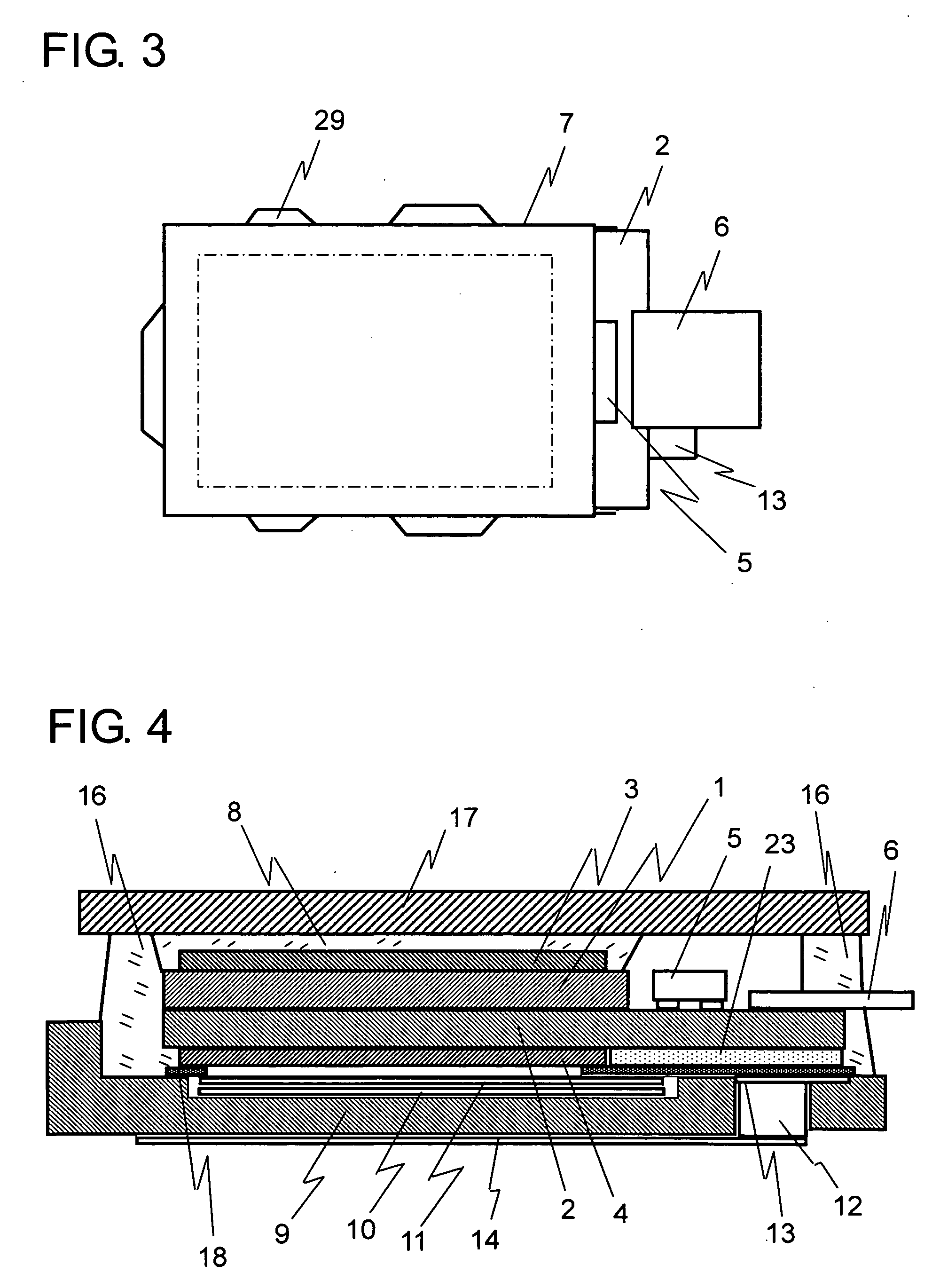
[0050]Hereinafter, a description is given of a second embodiment of the present invention with reference to FIGS. 4 to 6. FIG. 4 schematically illustrates a cross-sectional structure of a second embodiment. FIG. 5 is a top perspective view schematically illustrating a backlight used in the second embodiment. FIG. 6 is a top view illustrating the second embodiment. The second embodiment is different from the first embodiment in the detailed structure of the backlight and the position of the adhesive 16 that is disposed on the outer periphery of the liquid crystal panel. The duplicated description of the first embodiment such as the structure of the liquid crystal panel is appropriately omitted.

[0051]A touch panel 17 is bonded to the entire surface of the display side of the liquid crystal panel with the optical adhesive 8. The touch panel has various systems and various structures. In this embodiment, PET films on which transparent conductive films are formed face each other. Further...

third embodiment

[0058]Hereinafter, a description is given of a third embodiment of the present invention with reference to FIG. 7. FIG. 7 is a diagram schematically illustrating a cross-sectional structure of the third embodiment. The third embodiment is different from the second embodiment in the detailed structure of the backlight. The duplicated descriptions of the first and second embodiments are appropriately omitted.

[0059]The entire surface of the touch panel 17 adheres to the display surface side of the liquid crystal panel with the optical adhesive 8. The backlight includes the second film substrate 13 on which the LED 12 is mounted, the light guide plate 9, and a frame 19. The frame 19 is made of white polycarbonate, and has an opening into which the light guide plate is fitted. The frame 19 and the liquid crystal panel are fixed to each other with the adhesion material 15. In this embodiment, a double-faced adhesive tape is used as the adhesion material to fix the liquid crystal panel and...


PUM

PropertyMeasurementUnit
viscosityaaaaaaaaaa
thicknessaaaaaaaaaa
thicknessaaaaaaaaaa

Abstract

To solve deterioration of an impact resistance caused in a thinned liquid crystal panel, a display device includes a display panel held between a transparent plate arranged on a display surface side and a plate-like member on a rear surface side in a sandwiched manner, and the transparent plate and the plate-like member are bonded and fixed to each other with an adhesive (16) in an outer periphery of the display panel.

Description

BACKGROUND OF THE INVENTION[0001]1. Field of the Invention[0002]The present invention relates to a display device including a thin display panel. More particularly, the present invention relates to a reinforced structure of a display device in which a display panel is sandwiched between a plate member and a protective plate or a touch panel disposed on a display surface side. For example, the present invention is applicable to portable electronic devices such as a cellular phone, a PDA, or an electronic dictionary, and a display device thereof. Examples of the thin display panel include a liquid crystal display device of a passive matrix system, which uses an STN or TN liquid crystal, a liquid crystal display device of an active matrix system that drives the TN liquid crystal by a TFT element in a VA mode or an IPS mode, an organic EL display, and a plasma display.[0003]2. Description of the Related Art[0004]A liquid crystal panel has been known as a typical thin display panel. The ...

Claims


Application Information

Patent Timeline
Patent Type & Authority Applications(United States)
IPC IPC(8): G02F1/1333H05K5/00
CPCG02B6/005G02B6/0055G02F2201/503G02F1/133308G02F2001/133331G02B6/0093G02F1/133615G02F1/133331
Inventor MATSUHIRA, TSUTOMUICHINO, MASAYUKIHASHIZUME, ISAMUKAGAYA, YOICHI
Owner DAWNCREST IP LLC
Why Eureka
Try Eureka