Method for arranging print head chips

a print head and chip technology, applied in the direction of printing, inking apparatus, inspection/indentification of circuits, etc., can solve the problems of difficult to reduce in size, complex mechanical mechanism of laser printer head, etc., to achieve good linearity, good space arrangement precision, and high resolution

Inactive Publication Date: 2009-07-30
UNIVERSAL SCIENTIFIC INDUSTRIAL (SHANGHAI) CO LTD
View PDF2 Cites 13 Cited by
  • Summary
  • Abstract
  • Description
  • Claims
  • Application Information

AI Technical Summary

Benefits of technology

[0023]Therefore, because the method of the present invention is step by step and mate with accurate chip cutting technology, the print head such as the LED print head or the inkjet print head manufactured by above-mentioned method has a good linearity and good space arrangement precision. Moreover, the method of the present invention can achieve high resolution with 600-1200 dpi without doing position compensation.
[0024]Hence, the method of the present invention can solve the problem of low linearity of the prior art and increase the precision of color trap. In addition, the method of the present invention does not need the follow-up step of printing test and verifying print quality, so the method has a low cost and a high print quality.

Problems solved by technology

However, a laser printer head of the prior art has many optical components, and the mechanism of the laser printer head is complex and the optical path of the laser printer head is very longer.
Hence, the optical structure is quite complex and difficult to reduce in size for using a laser in this way.
1. An offset along an x-direction between the first LED spot d1a on a substrate ba and a last LED spot d192a on the substrate ba is about 211 μm±300 μm. In other words, a maximum offset Xn along the x-direction between the first LED spot d1a and the last LED spot d192a is 300 μm. In addition, with regard to the prior art with the size of A4 and the resolution of 600 dpi, a distance of each spot is about 42.3 μm. Hence, the distance of the maximum offset Xn along the x-direction is about 7 spot (300 / 42.3=7.09) in the prior art.
2. A maximum offset Yn along a y-direction between the first LED spot d1a on the substrate ba and the last LED spot d192a on the substrate ba is 150 μm. In addition, with regard to the prior art with the size of A4 and the resolution of 600 dpi, a distance of each spot is about 42.3 μm. Hence, the distance of the maximum offset Yn along the y-direction is about 3.5 spot (150 / 42.3=3.54) in the first embodiment.
However, no matter which solve method is used in the prior art, abovementioned steps such as measuring LED spots and position compensation and the follow-up step of printing test and verifying print quality need to pay large cost.

Method used


Image

  • Method for arranging print head chips
  • Method for arranging print head chips
  • Method for arranging print head chips

Examples


Embodiment Construction

[0031]The present invention provides a method for arranging print head chips, including:

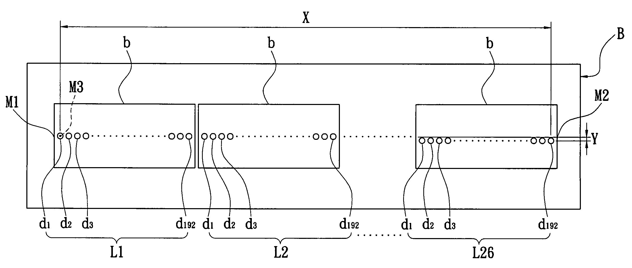
[0032]Step (a): setting a first fiducial mark and a second fiducial mark on a PCB for determining coordinate positions of a plurality of array units that are arranged on the PCB and calculating a print range of the array units, and each array unit having a plurality of spots that are transversely arranged from the first one of the spots to the last one of the spots in sequence;

[0033]Step (b): setting a third fiducial mark as a start point for arranging the first spot of a first array unit of the array units on the PCB; and

[0034]Step (c): arranging other array units on the PCB in sequence according to the coordinate positions and the start point in order to finish the manufacture of a print head with high print quality. In addition, the print head with high print quality can be an LED print head (LPH) applied to an EPG (Electrophotography) printer or an inkjet print head applied to an inkjet print...


PUM

PropertyMeasurementUnit
widthaaaaaaaaaa
distanceaaaaaaaaaa
sizeaaaaaaaaaa

Abstract

A method for arranging print head chips, includes: (a) setting a first fiducial mark and a second fiducial mark on a PCB for determining coordinate positions of a plurality of array units that are arranged on the PCB and calculating a print range of the array units, wherein each array unit has a plurality of spots that are transversely arranged from the first one of the spots to the last one of the spots in sequence; (b) setting a third fiducial mark as a start point for arranging the first spot of a first array unit of the array units on the PCB; and (c) arranging other array units on the PCB in sequence according to the coordinate positions and the start point.

Description

BACKGROUND OF THE INVENTION[0001]1. Field of the Invention[0002]The present invention relates to a method for arranging print head chips, and particularly relates to a method of arranging print head chips using a single arrangement start point in order to obtain a print head with high print quality.[0003]2. Description of the Related Art[0004]In the typical printer technology, a laser is used as a light source in a printer head to scan and transfer the printing information as light signals to a rotating drum in order to generate electrostatic latent images formed on the rotating drum. Moreover, the printing method further includes a toner absorbing step, a transferring step, a hot pressing step, an electrostatic discharging step etc. to achieve printing requirement. However, a laser printer head of the prior art has many optical components, and the mechanism of the laser printer head is complex and the optical path of the laser printer head is very longer. Hence, the optical structu...

Claims


Application Information

Patent Timeline
Patent Type & Authority Applications(United States)
IPC IPC(8): B41J2/45B41J2/145H05K3/30B41J2/16
CPCB41J2/145B41J2/45B41J2202/19B41J2202/20H05K1/0269Y10T29/49401H05K3/328H05K2201/09918H05K2201/10106H05K2203/049Y10T29/4913H05K3/303
Inventor WU, MING-CHE
Owner UNIVERSAL SCIENTIFIC INDUSTRIAL (SHANGHAI) CO LTD
Why Eureka
Try Eureka