Phosphorescent OLED having double hole-blocking layers

a technology of phosphorescent oled and hole-blocking layer, which is applied in the direction of luminescent compositions, electrical devices, chemistry apparatus and processes, etc., can solve the problems of difficult to find or design such a hole-blocking material, and one hbl cannot fully improve the device performan

Inactive Publication Date: 2009-07-30
GLOBAL OLED TECH
View PDF64 Cites 94 Cited by
  • Summary
  • Abstract
  • Description
  • Claims
  • Application Information

AI Technical Summary

Benefits of technology

[0020]The present invention forms two adjacent HBLs between the LEL and the cathode to enhance hole- and exciton-blocking effects as well as to enhance electron injection capability in the device. It is an advantage of the present invention that the phosphorescent OLED having two hole-blocking layers can generate electrophosphorescence with improved external quantum efficiency and operational lifetime.
that the phosphorescent OLED having two hole-blocking layers can generate electrophosphorescence with improved external quantum efficiency and operational lifetime.

Problems solved by technology

Although an HBL between a phosphorescent LEL and an ETL can effectively block holes (excitons) from transporting (diffusing) into the ETL, and can increase external quantum efficiency in a phosphorescent OLED, it has been found that only one HBL cannot fully improve device performance.
However, in real applications, it is difficult to find or to design such an effective hole-blocking material.

Method used


Image

  • Phosphorescent OLED having double hole-blocking layers
  • Phosphorescent OLED having double hole-blocking layers
  • Phosphorescent OLED having double hole-blocking layers

Examples


examples

[0289]The following examples are presented for a further understanding of the present invention. The reduction potential and the oxidation potential of the materials were measured using a Model CHI660 electrochemical analyzer (CH Instruments, Inc., Austin, Tex.) with the method as discussed before. During the fabrication of OLEDs, the thickness of the organic layers and the doping concentrations were controlled and measured in situ using calibrated thickness monitors built in an evaporation system (Made by Trovato Mfg., Inc., Fairport, N.Y.). The EL characteristics of all the fabricated devices were evaluated using a constant current source (KEITHLEY 2400 SourceMeter, made by Keithley Instruments, Inc., Cleveland, Ohio) and a photometer (PHOTO RESEARCH SpectraScan PR 650, made by Photo Research, Inc., Chatsworth, Calif.) at room temperature. Operational lifetime (or stability) of the devices was tested at the room temperature and at an initial luminance of 1,000 cd / m2 by driving a c...

examples 1-3

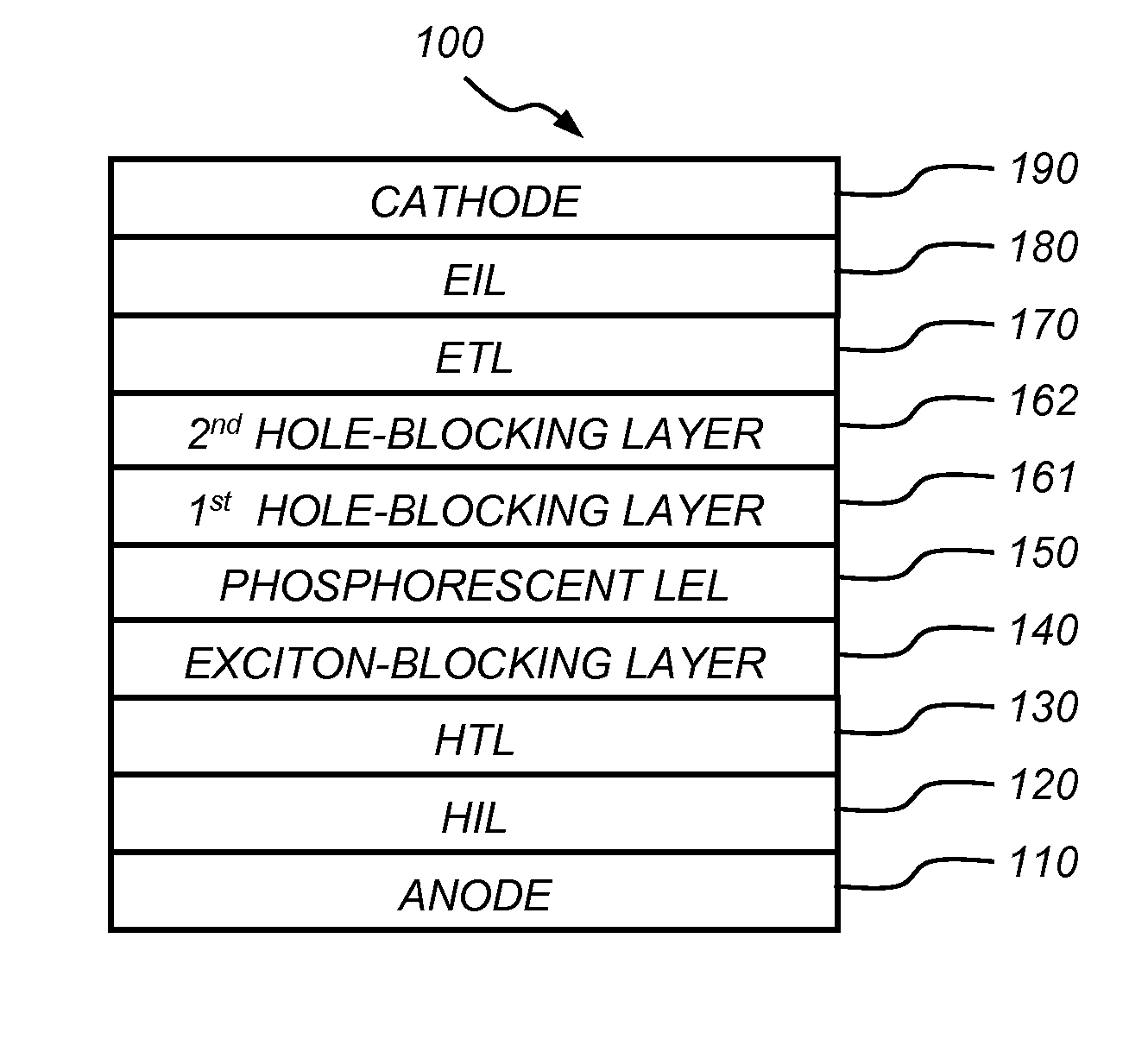
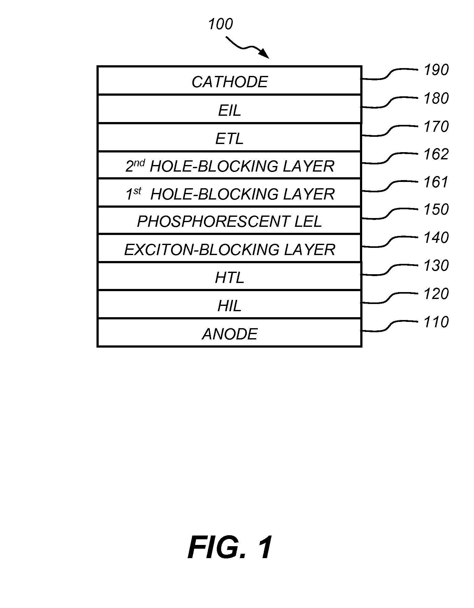
[0290]The preparation of a conventional OLED (Device 1) is as follows: A ˜1.1 mm thick glass substrate coated with a transparent ITO conductive layer was cleaned and dried using a commercial glass scrubber tool. The thickness of ITO is about 22 nm and the sheet resistance of the ITO is about 68 Ω / square. The ITO surface was subsequently treated with oxidative plasma to condition the surface as an anode. A layer of CFx, 1 nm thick, was deposited on the clean ITO surface as the anode buffer layer by decomposing CHF3 gas in an RF plasma treatment chamber. The substrate was then transferred into a vacuum deposition chamber for deposition of all other layers on top of the substrate. The following layers were deposited in the following sequence by evaporation from a heated boat under a vacuum of approximately 10−6 Torr:

[0291]a) a HTL, 100 nm thick, including N,N′-di-1-naphthyl-N,N′-diphenyl-4,4′-diaminobiphenyl (NPB);

[0292]b) an EXBL, 10 nm thick, including 4-(9H-carbazol-9-yl)-N,N-bis[4-...

examples 4-5

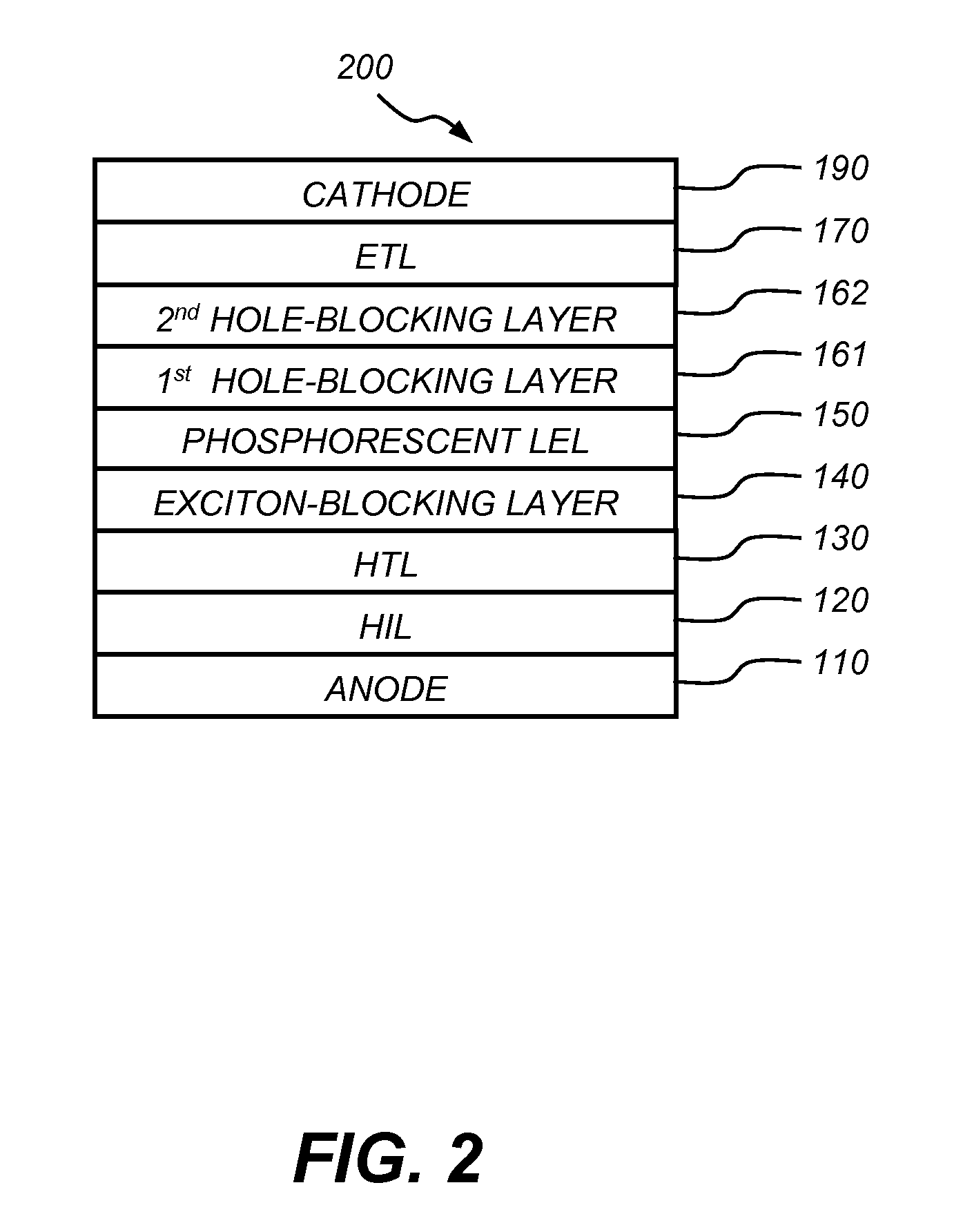
[0321]A comparative phosphorescent OLED (Device 4) is fabricated with the same method and the same layer structure as Example 1.

[0322]Device 4 is denoted as: ITO / 100 nm NPB / 10 nm TCTA / 20 nm CBP:6% Ir(ppy)3 / 25 nm Bphen / 15 nm Bphen:1.0% Li / 100 nm Al. The EL performance of the device is summarized in Table 1.

[0323]An inventive phosphorescent OLED (Device 5) is fabricated with the same method and the same layer structure as Example 4, except that the there are two HBLs in the device. The layer structure is:

[0324]a) a HTL, 100 nm thick, including NPB;

[0325]b) an EXBL, 10 nm thick, including TCTA;

[0326]c) a LEL, 20 nm thick, including CBP doped with 6% of Ir(ppy)3 by volume;

[0327]d) a first HBL, 5 nm thick, including Formula (X-1) (HOMO energy <−6.1 eV, LUMO energy=−2.73 eV, triplet energy=2.95 eV);

[0328]e) a second HBL, 20 nm thick, including Bphen;

[0329]f) an ETL, 15 nm thick, including Bphen doped with about 1.0% of lithium; and

[0330]g) a cathode: approximately 100 nm thick, including ...


PUM

PropertyMeasurementUnit
thicknessaaaaaaaaaa
thicknessaaaaaaaaaa
thickaaaaaaaaaa

Abstract

An organic light-emitting device has a first hole-blocking layer in contact with a phosphorescent light-emitting layer and a second hole-blocking layer in contact with the first. The material in the first hole-blocking layer has a triplet energy greater than the host of the phosphorescent layer and the material in the second hole-blocking layer has a triplet energy higher than the dopant in the phosphorescent layer. Both hole-blocking materials have lower HOMO energies than the host of the phosphorescent light-emitting layer

Description

CROSS REFERENCE TO RELATED APPLICATION[0001]Reference is made to commonly assigned U.S. patent application Ser. No. 11 / 924,635 filed Oct. 26, 2007, entitled “Phosphorescent OLED Device With Certain Fluoranthene Host” by Begley et al, the disclosure of which is herein incorporated by reference.FIELD OF THE INVENTION[0002]The present invention relates to organic light-emitting devices (OLEDs) or organic electroluminescent (EL) devices including a phosphorescent light-emitting layer and two adjacent hole-blocking layers.BACKGROUND OF THE INVENTION[0003]Organic light-emitting devices (OLEDs) or organic electroluminescent (EL) devices have been known for several decades, however, their performance limitations have represented a barrier for many applications. In the simplest form, an OLED is comprised of an anode for hole injection, a cathode for electron injection, and an organic medium sandwiched between these electrodes to support charge recombination and emission of light. Representat...

Claims


Application Information

Patent Timeline
Patent Type & Authority Applications(United States)
IPC IPC(8): C09K11/00B32B9/00
CPCH01L51/005H01L51/0081H01L51/5096H01L51/5016H01L51/5052H01L51/0085H10K85/60H10K85/324H10K85/342H10K50/11H10K2101/10H10K50/165H10K50/18H10K50/805H10K50/814H10K50/824
Inventor LIAO, LIANG-SHENGBEGLEY, WILLIAM J.PELLOW, CYNTHIA A.
Owner GLOBAL OLED TECH
Why Eureka
Try Eureka