

Method for Producing Silicon Wafer
- Summary
- Abstract
- Description
- Claims
- Application Information
AI Technical Summary
Benefits of technology
Problems solved by technology
Method used
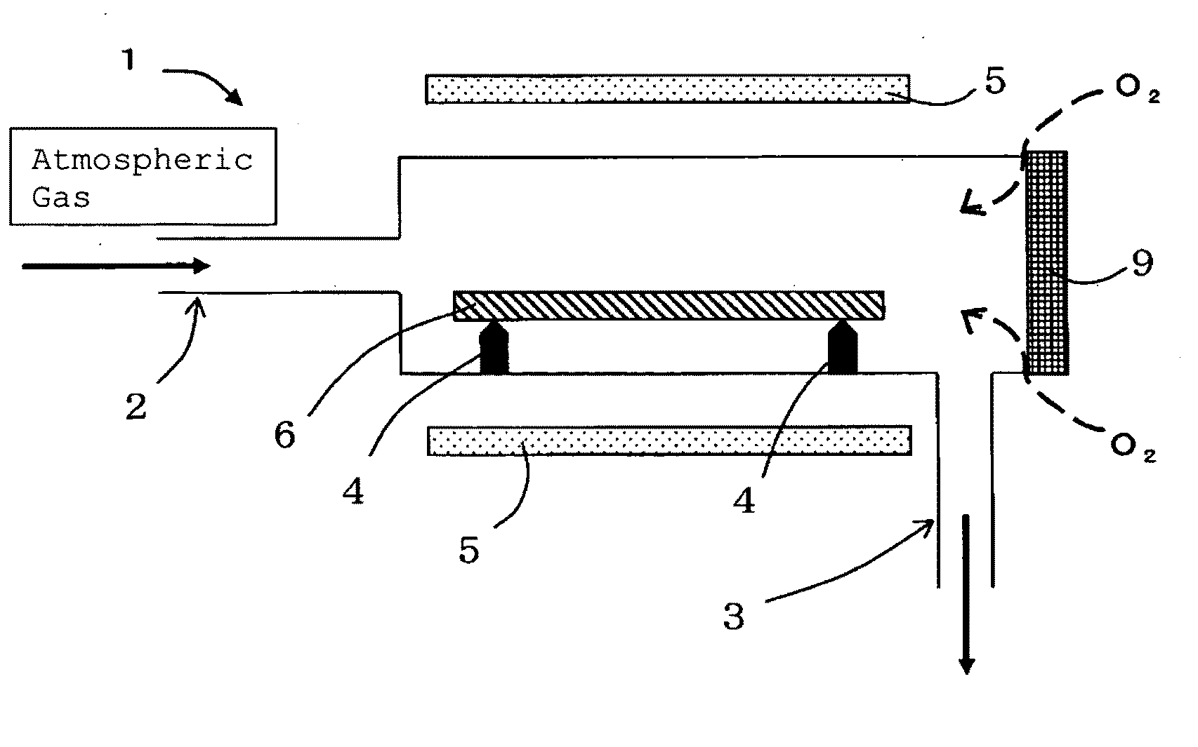
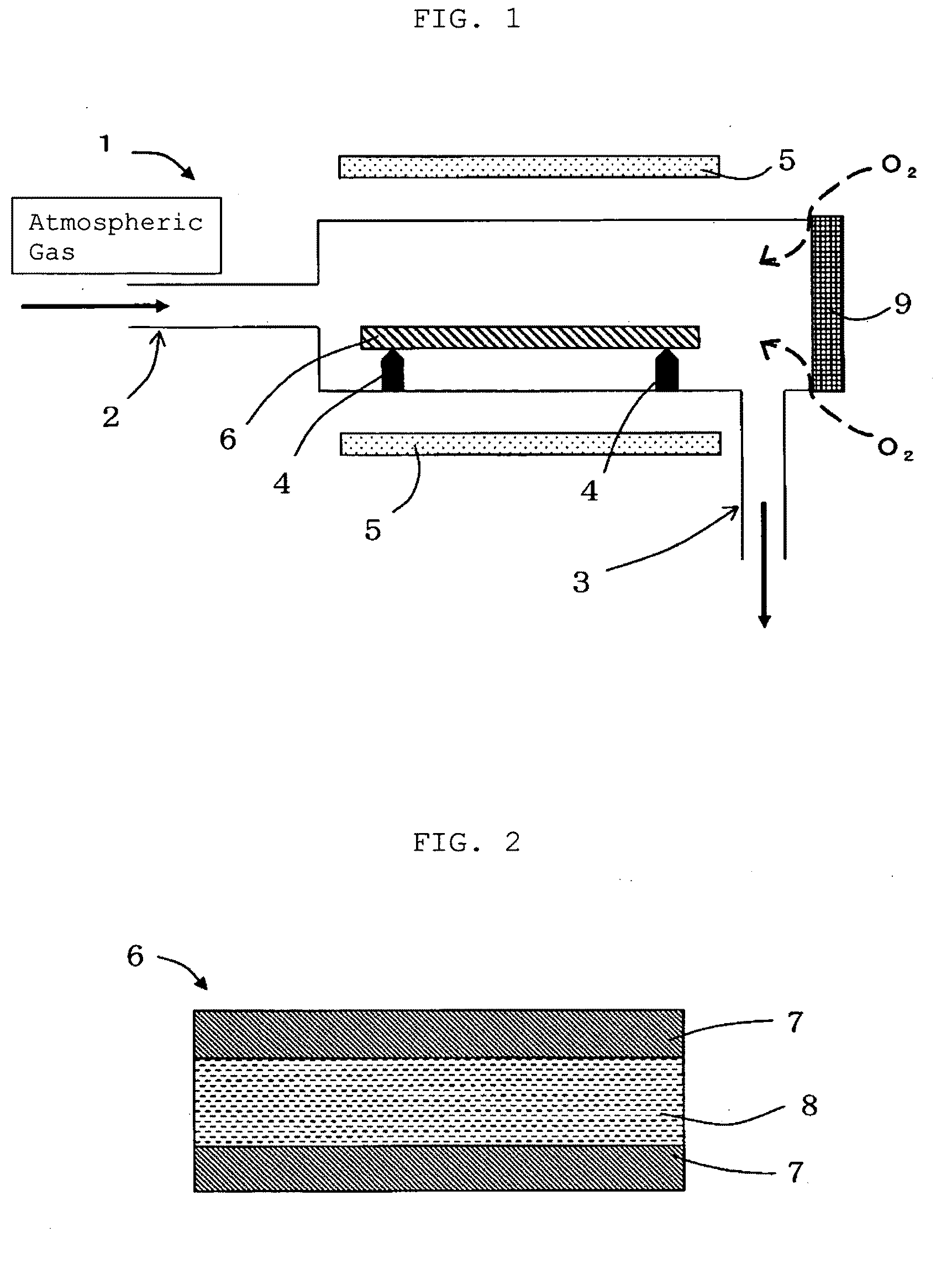
Image

Examples
example 1
[0047]By varying a concentration of oxygen mixed with nitrogen gas as atmospheric gas in the range of above 0 ppm and below 100 ppm, a silicon wafer was subject to RTA heat treatment at a temperature of 1200° C. for a time period of 10 seconds, 30 seconds and 60 seconds, respectively. Then, heat treatment for oxygen precipitation was performed and residual Oi before and after the heat treatment for oxygen precipitation was measured so as to investigate the amount of precipitated oxygen.
[0048]The result is shown in FIG. 5. It is apparent from the graph that the amount of precipitated oxygen was increased if the concentration of the oxygen mixed in the nitrogen gas atmosphere was in the range of 15 ppm to 90 ppm. It is also apparent that with longer time period of RTA heat treatment, the amount of precipitated oxygen was increased. Especially, the obtained amount of precipitated oxygen could be tripled in the case of mixed amount of oxygen being 50 ppm, the temperature being 1200° C. ...
example 2
[0049]A silicon wafer was subject to RTA heat treatment, in which oxygen at a concentration of 25 ppm was mixed with nitrogen gas as atmospheric gas.
[0050]The RTA heat treatment here was performed under a condition of temperature of 1200° C. and of a time period of 10 seconds.
[0051]Next, for investigating a BMD zone formed by the subsequent heat treatment, three-stage heat treatment was performed so as to measure BMD density.
[0052]When an oxynitride film formed on the surface of the silicon wafer through RTA heat treatment was observed by XRT, it was apparent that the oxynitride film was formed on the entire surface of the silicon wafer (See FIG. 4(B)).
[0053]The BMD zone formed inside the silicon wafer after the three-stage heat treatment is shown in FIG. 7(B). BMD density was measured, and the result is shown in FIG. 6.
example 3
[0054]A silicon wafer was subject to RTA heat treatment, in which oxygen at a concentration of 50 ppm was mixed with nitrogen gas as atmospheric gas.
[0055]The RTA heat treatment here was performed under a condition of temperature of 1200° C. and of a time period of 10 seconds.
[0056]Next, for investigating a BMD zone formed by the subsequent heat treatment, three-stage heat treatment was performed so as to measure BMD density.
[0057]When an oxynitride film formed on the surface of the silicon wafer through RTA heat treatment was observed by XRT, it was apparent that the oxynitride film was formed almost on the entire surface of the silicon wafer (See FIG. 4(C)).
[0058]The BMD zone formed inside the silicon wafer after the three-stage heat treatment is shown in FIG. 7(C). BMD density was measured, and the result is shown in FIG. 6.
PUM
 Abstract
Description
Claims
Application Information