Method of bonding, thinning, and releasing wafer

a technology of thinning and releasing wafers, applied in the directions of transportation and packaging, paper/cardboard containers, containers, etc., can solve the problems of affecting the yield of thinned wafers, the inability to support thinned wafers only on protection tapes, and the inability to automate processing steps, so as to reduce the risk of damaging the wafers and the yield of higher yield

Inactive Publication Date: 2009-08-13
TOKYO OHKA KOGYO CO LTD
View PDF5 Cites 17 Cited by
  • Summary
  • Abstract
  • Description
  • Claims
  • Application Information

AI Technical Summary

Benefits of technology

[0035]Also, after the thinning process, a release agent is used to dissolve the adhesive layers in order to release the wafer so that needless effects such as the effects of heat or the like are not applied to the circuit formation surface of the wafer from the external environment, resulting in a lower risk of damaging the wafer and a higher yield.

Problems solved by technology

However, in this method, breaks or cracks off are often made in a wafer when protection tape is peeled from the wafer.
Further, a thinned wafer cannot be supported only on protection tape.
Accordingly, processing steps cannot be automated.
However, this method uses a thermoplastic film that has been dried as an adhesive agent for bonding a protection substrate and a thermoplastic film, and thus a heating step has to be performed in order to soften the thermoplastic film when releasing the wafer from the protection substrate.
Softening a thermoplastic film that has been dried requires a high temperature, posing a high risk that circuits on a wafer may be damaged.
Further, the use of film adhesive causes a variation among portions in bonding strength so that some portions may be peeled when being polished and other portions may be difficult to be released when a wafer is released from the protection substrate, which are problematic.
In order to prevent such transfers, anti-transfer sheets are used; however, the use of such sheets does not prevent the transfer of the through-hole pattern completely.
However, too hard an adhesive agent layer can cause a decrease in the bonding property, allowing the periphery of the wafer that has been thinned through grinding and polishing to be released and peeled from the adhesive agent layer.
This causes a problem wherein the bonding property of an adhesive agent layer that is too hard is low.
Accordingly, the thickness, material, and hardness, etc. of an adhesive agent have to be sufficiently adjusted in accordance with the thickness of the polished wafer, which is troublesome.

Method used


Image

  • Method of bonding, thinning, and releasing wafer
  • Method of bonding, thinning, and releasing wafer
  • Method of bonding, thinning, and releasing wafer

Examples


example 1

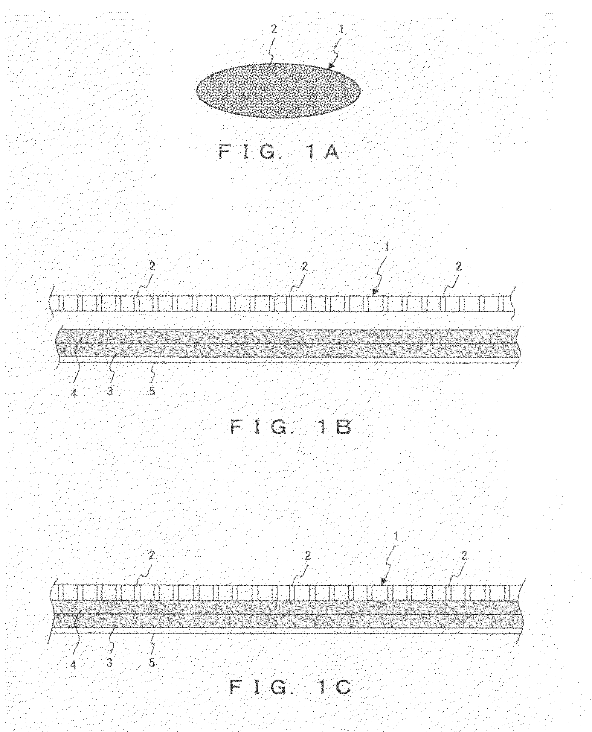
[0075]FIG. 1A is a perspective view schematically showing a configuration of a support plate used in a process of thinning a wafer executed in example 1. This process will be explained later. FIG. 1B is a cross-sectional view schematically showing the relationship between the support plate and the wafer when they are aligned with each other. FIG. 1C is a cross-sectional view schematically showing the state of the support plate and the wafer after they are bonded together by a thermal compression bonding method with an adhesive agent layer between them.

[0076]As shown in FIG. 1A, a support plate 1 is a rigid-body circular glass plate.

[0077]As shown in FIG. 1A, a number of micro through holes 2 are formed evenly throughout the entire surface of the support plate 1.

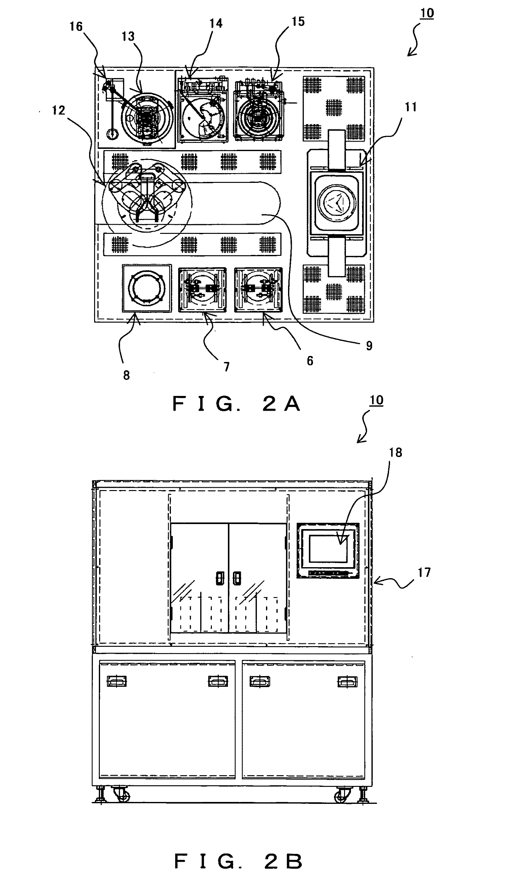
[0078]As shown in FIG. 2B, the support plate 1 is aligned with a wafer 5 in an adhering apparatus. A plurality of types of adhesive agent layers including hard and soft types (a hard adhesive agent layer 3 and a soft adhesive...

example 2

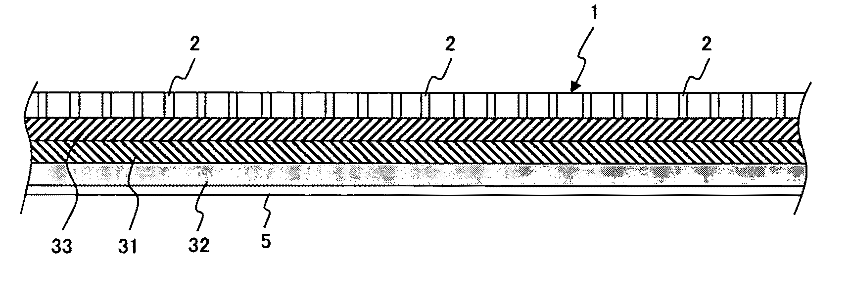
[0131]FIG. 6 is a cross-sectional view schematically showing a state of a support plate and wafer that have been bonded with adhesive agent layers between them by a thermal compression bonding method, which is executed before the wafer is thinned by being ground / polished in the process of thinning a wafer explained in example 2.

[0132]As shown in FIG. 6, the support plate 1 and the wafer 5 are bonded together with three layers, i.e., a hard adhesive agent layer 31 between soft adhesive agent layers 32 and 33.

[0133]One of the two soft adhesive agent layers is bonded to the wafer 5 (the soft adhesive agent layer 32 at the bottom in FIG. 6), and the other of the soft adhesive agent layers is bonded to the support plate 1 (the soft adhesive agent layer 33 at the top in FIG. 6).

[0134]It is possible to apply the above three adhesive agent layers by repeating steps S1 and S2 shown in FIG. 3. It is also possible to first apply the soft adhesive agent layer 32 and thereafter stack sheets of t...


PUM

PropertyMeasurementUnit
diameteraaaaaaaaaa
thicknessaaaaaaaaaa
thicknessaaaaaaaaaa

Abstract

An adhesive agent layer for bonding a support plate (1) and a wafer (5) is in a three-layer configuration in which a hard layer (31) is sandwiched between soft layers (32) and (33) from above and below. Both the top and bottom surfaces of the adhesive agent layer are soft adhesive agent layers, which results in an excellent bonding affinity with the wafer 5 and the support plate (1). Accordingly, the peripheral portion of the wafer (5) can be prevented from being lifted before a dicing process. Further, because the sandwiched adhesive agent layer is the hard adhesive agent layer (31), even when the non-adhesive surface of the support plate (1) is vacuum suctioned, or when a pressure is applied from a grinder, the hard adhesive agent layer (31) is not deformed according to the soft adhesive agent layer (33) being drawn or pushed into through holes (2).

Description

TECHNICAL FIELD[0001]The present invention relates to a method by which a wafer is bonded to a support plate before the wafer is thinned by being ground and polished, to a method of thinning the wafer, and to a method of releasing the wafer.BACKGROUND ART[0002]Portable electronic devices such as IC cards, mobile phones, digital cameras, etc. are widely used. In recent years, there has been demand for all of these devices to become thinner, smaller, and lighter without exception.[0003]In order to meet this demand, semiconductor chips used in these devices must also become thinner.[0004]It has been said that the thickness of silicon wafers (simply referred to as a wafer or wafer chips hereinafter) used to produce semiconductor chips must be reduced to between 25 μm and 50 μm for the next-generation semiconductor chips, while the current wafer thickness is between 125 μm and 150 μm.[0005]In the conventional methods of thinning wafers, protection tape is applied on the circuit formed su...

Claims


Application Information

Patent Timeline
Patent Type & Authority Applications(United States)
IPC IPC(8): B32B38/00B32B37/14B32B38/10
CPCC09J5/04C09J2203/326H01L21/67132H01L21/6835Y10T156/10H01L21/78H01L2221/68327H01L2221/68381H01L2221/68318H01L21/6836
Inventor INAO, YOSHIHIRO
Owner TOKYO OHKA KOGYO CO LTD
Why Eureka
Try Eureka