Via in via circuit board structure

a circuit board and via technology, applied in the field of circuit board technology, can solve the problems of electrical signal loss and noise of electric signals that use vias to pass through ground and/or power signal layers of circuit boards, ground and power planes may include a large amount of electrical noise, and noise may be undesirabl

Inactive Publication Date: 2009-08-13
AVAGO TECH WIRELESS IP SINGAPORE PTE
View PDF7 Cites 37 Cited by
  • Summary
  • Abstract
  • Description
  • Claims
  • Application Information

AI Technical Summary

Problems solved by technology

However, electrical signals that use vias to pass through ground and / or power signal layers of a circuit board frequently suffer from electrical signal loss and noise.
Ground and power planes may include a large amount of electrical noise due to circuit switching and other circuit functions.
This noise may be undesirably coupled onto the electrical signals passing through the ground or power planes on vias.
This problem is especially acute for single ended signals, which have less ability to reject noise than differential signals.

Method used


Image

  • Via in via circuit board structure
  • Via in via circuit board structure
  • Via in via circuit board structure

Examples


embodiments

EXAMPLE VIA-IN-VIA-EMBODIMENTS

[0035]Example embodiments are described for providing electrical connections through circuit boards. For example, electrical connections are made through circuit boards using novel via structures. The example embodiments described herein are provided for illustrative purposes, and are not limiting. Further structural and operational embodiments, including modifications / alterations, will become apparent to persons skilled in the relevant art(s) from the teachings herein.

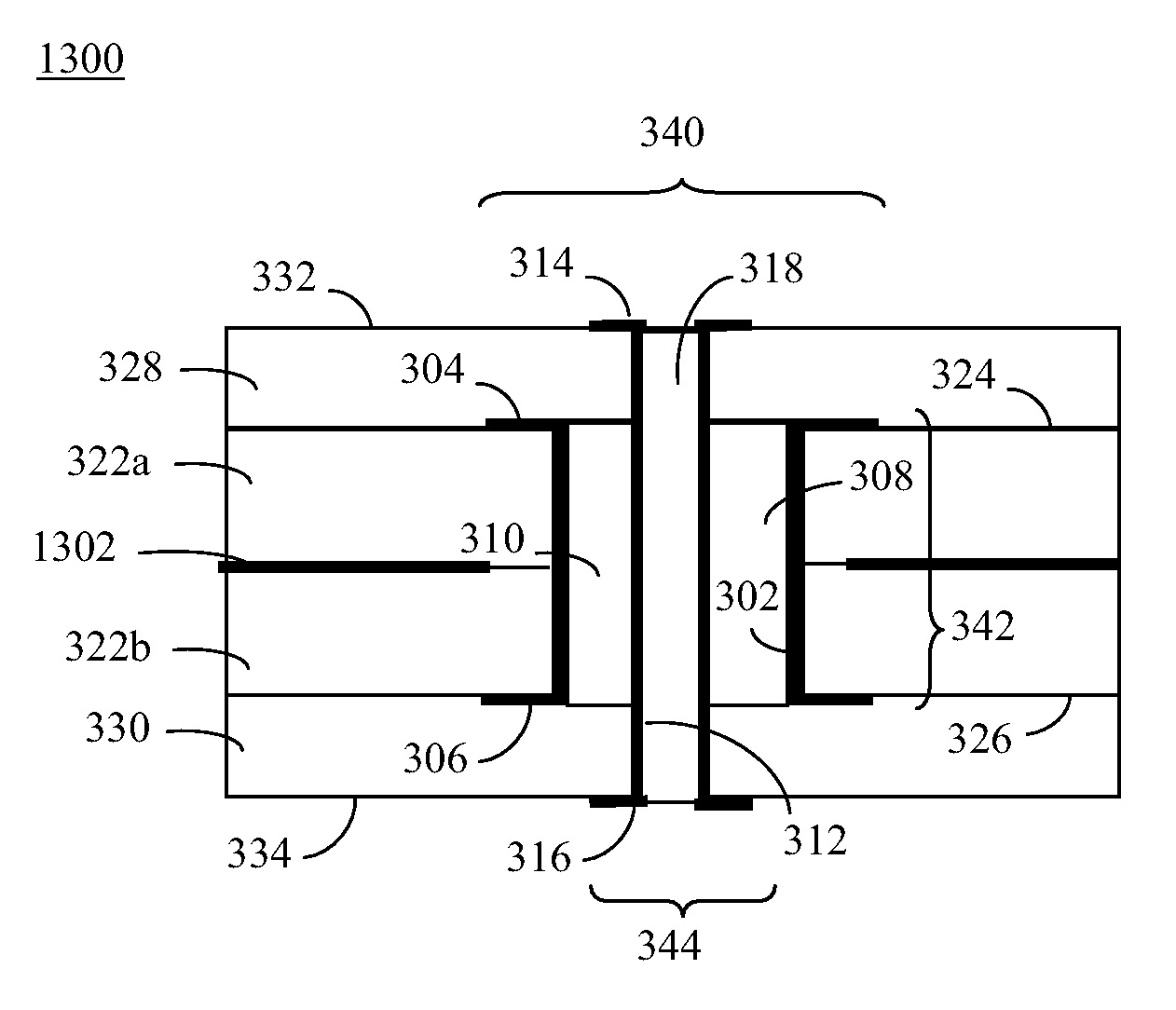
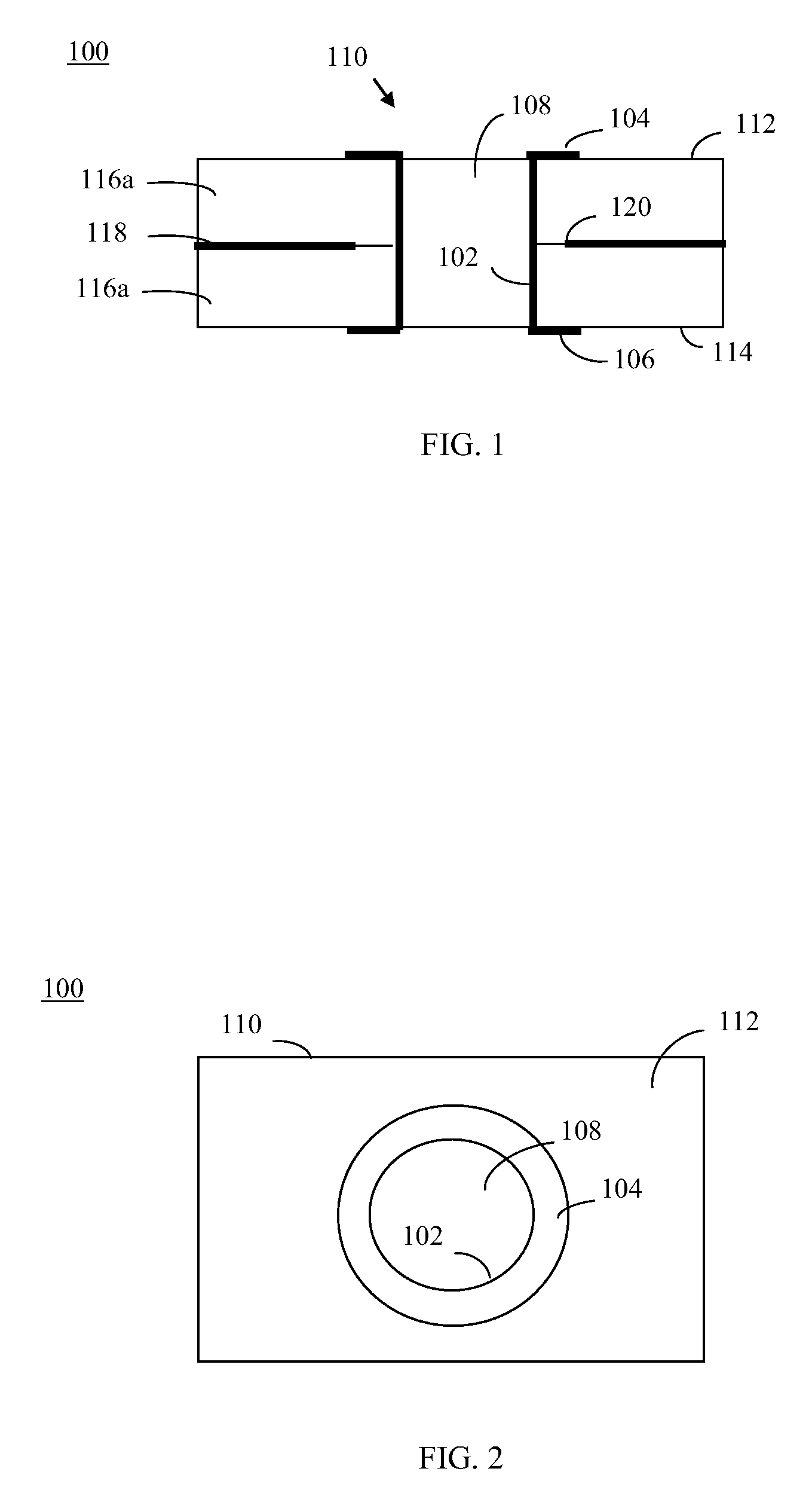
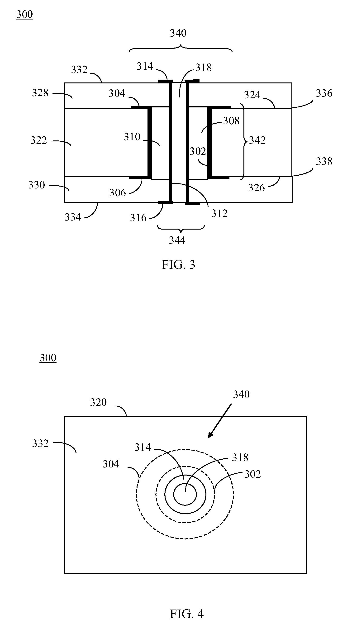
[0036]In embodiments, a via-in-via structure includes a second via that is formed in a first via. The first and second vias provide a pair of electrical signal paths through a circuit board. In this manner, two related or unrelated electrical signals may be passed through the circuit board by the via-in-via structure. In one example, a differential signal pair may be conducted through the circuit board using the via-in-via structure. Alternatively, an electrical signal and an associated g...


PUM


Abstract

Methods, systems, and apparatuses for electrical connections through circuit boards are described. A via-in-via structure in a circuit board provides two electrical signal paths. The circuit board includes a dielectric layer having opposing first and second planar surfaces. A first opening extends through the dielectric layer. An electrically conductive coating coats a surface of the dielectric layer in the first opening. An electrically insulating material substantially fills the first opening. The circuit board includes a first additional dielectric layer attached to the first planar surface, and a second additional dielectric layer attached to the second planar surface. A second opening extends through the first additional dielectric layer, the electrically insulating material filling the first opening, and the second additional dielectric layer. An electrically conductive material coats a surface of the first additional dielectric layer, the electrically insulating material, and the second additional dielectric layer in the second opening.

Description

BACKGROUND OF THE INVENTION[0001]1. Field of the Invention[0002]The present invention relates to circuit board technology, and more particularly, to electrical connections through circuit boards.[0003]2. Background Art[0004]Various types of circuit boards exist, including printed circuit boards (PCBs) and substrates used in integrated circuit packages. A PCB mounts electronic components, and provides electrically conductive pathways to electrically connect the mounted electronic components. A substrate in an integrated circuit package mounts one or more integrated circuit chips, and provides electrical pathways from the mounted chip(s) to electrical mounting members (e.g., pins, pads, solder balls, etc.) for the package. The electrical mounting members are used to mount the package to another circuit board.[0005]A typical circuit board includes one or more layers of electrically conductive material laminated onto an electrically insulating substrate material. Multi-layer circuit boa...

Claims


Application Information

Patent Timeline
Patent Type & Authority Applications(United States)
IPC IPC(8): H01L23/535H01L21/44H01L21/4763H05K3/42
CPCH01L21/486H01L23/49816H01L2924/3025H01L2924/15311H01L2224/73265H01L2224/48227H01L2224/32225H05K2201/09809H05K3/4644H05K3/429H05K1/115H05K1/0222H01L23/49827H01L2924/00
Inventor ZHANG, TONGLONG
Owner AVAGO TECH WIRELESS IP SINGAPORE PTE
Why Eureka
Try Eureka