Laser processing method

a laser processing and laser technology, applied in the field of laser processing methods, can solve the problems of reducing the adhesive strength of the adhesive material, cracking or breaking, and reducing the die strength, so as to achieve reliable products and suppress overheating

Active Publication Date: 2009-08-13
DISCO CORP
View PDF11 Cites 17 Cited by
  • Summary
  • Abstract
  • Description
  • Claims
  • Application Information

AI Technical Summary

Benefits of technology

[0011]It is therefore an object of the present invention to provide a laser processing method which can suppress the overheating at a portion immediately before the intersection of each first street and each second street in applying a laser beam along each second street to form each second groove intersecting each first groove previously formed, thereby preventing the problem caused by this overheating to obtain reliable products.

Problems solved by technology

Further, the round corners of each chip 3 become weak to cause a reduction in die strength, resulting in cracking or breakage in some case.
In this respect, a UV (ultraviolet) curing type adhesive material is used as the adhesive layer formed on the dicing tape, and ultraviolet light is applied to the dicing tape in picking up each chip, thereby reducing the adhesive strength of the adhesive material.
However, in applying a laser beam along each second street after forming each first groove along each first street in the conventional dicing step, the portion of each second street immediately before reaching each first groove is overheated by the laser beam as mentioned above.
Accordingly, the UV curing type adhesive material of the dicing tape at this portion is deteriorated by the overheating, causing a problem such that the adhesive strength of the adhesive material is not reduced in spite of the application of ultraviolet light.
As a result, each chip is hard to peel off at this portion from the dicing tape in the pickup operation, thus reducing the easiness of the pickup operation.
This problem occurs both in the formation of a groove having a depth smaller than the thickness of the wafer and in the formation of a slit cut through the thickness of the wafer.

Method used


Image

  • Laser processing method
  • Laser processing method
  • Laser processing method

Examples


Embodiment Construction

[0025]A preferred embodiment of the present invention will now be described with reference to the drawings.

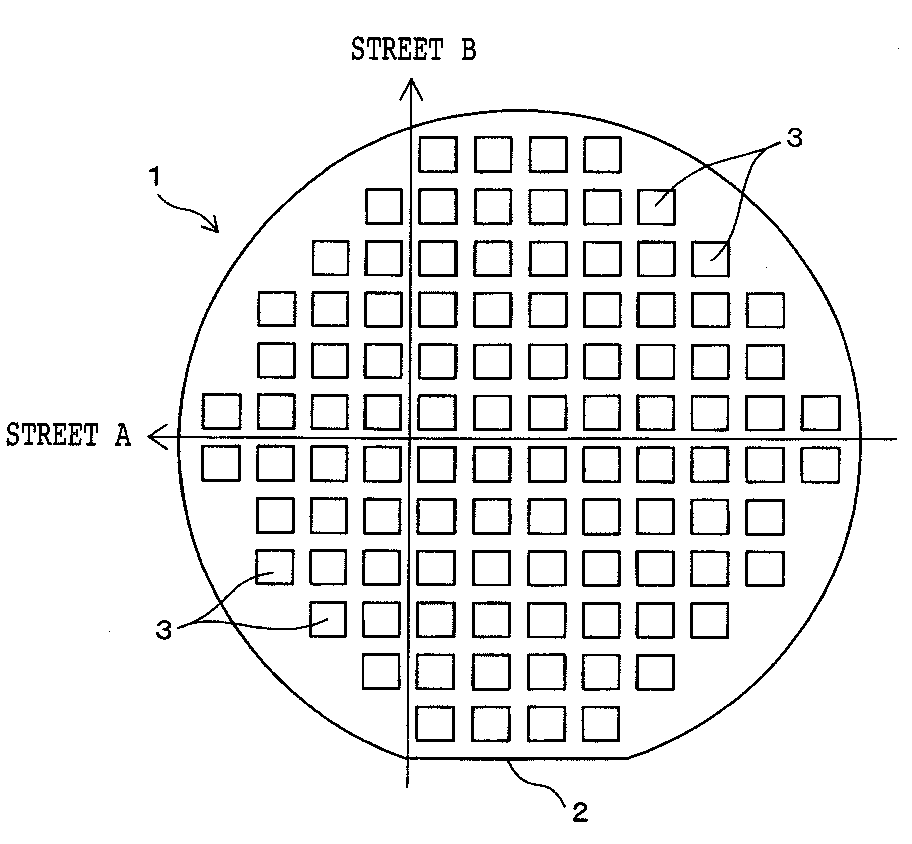
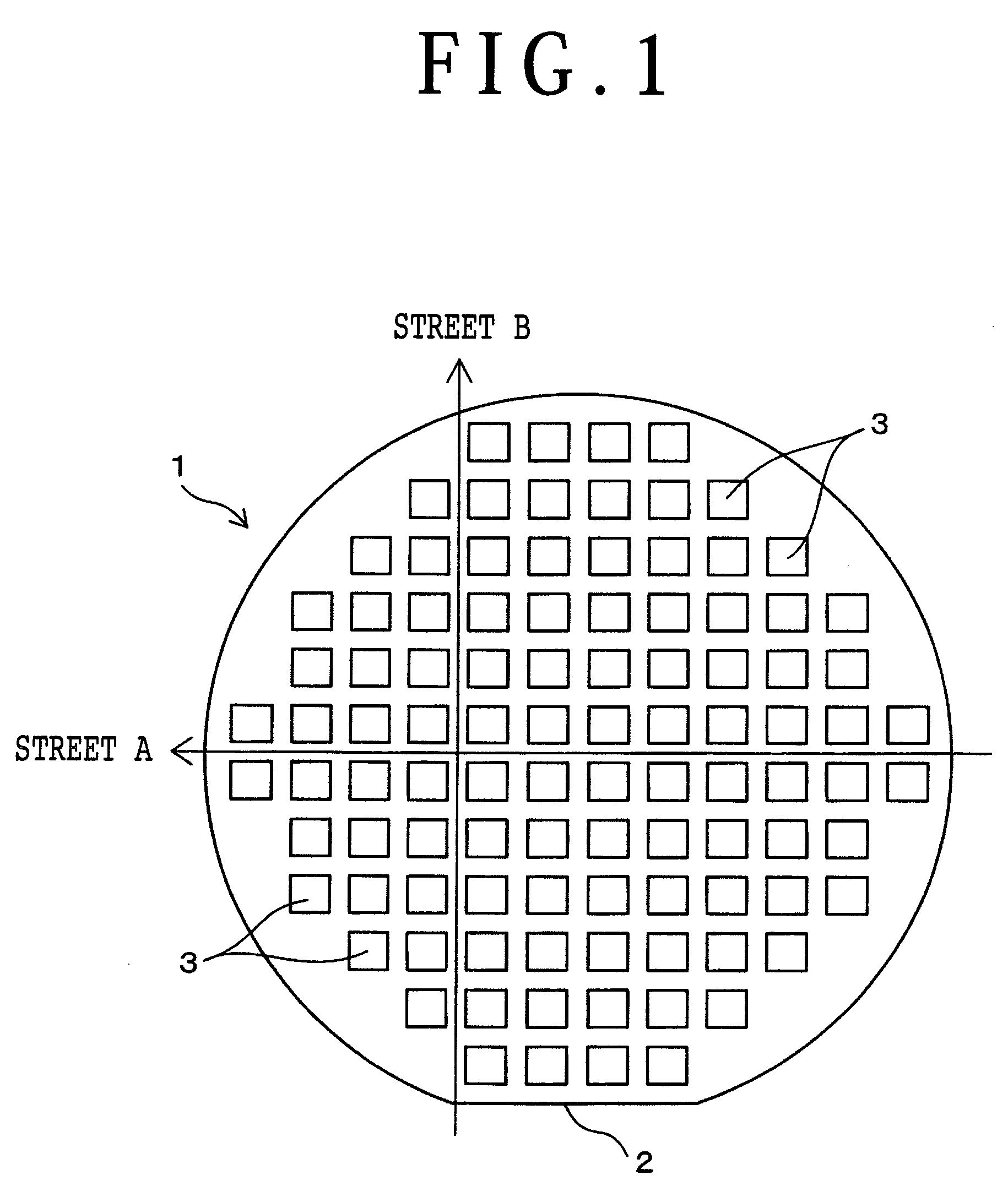
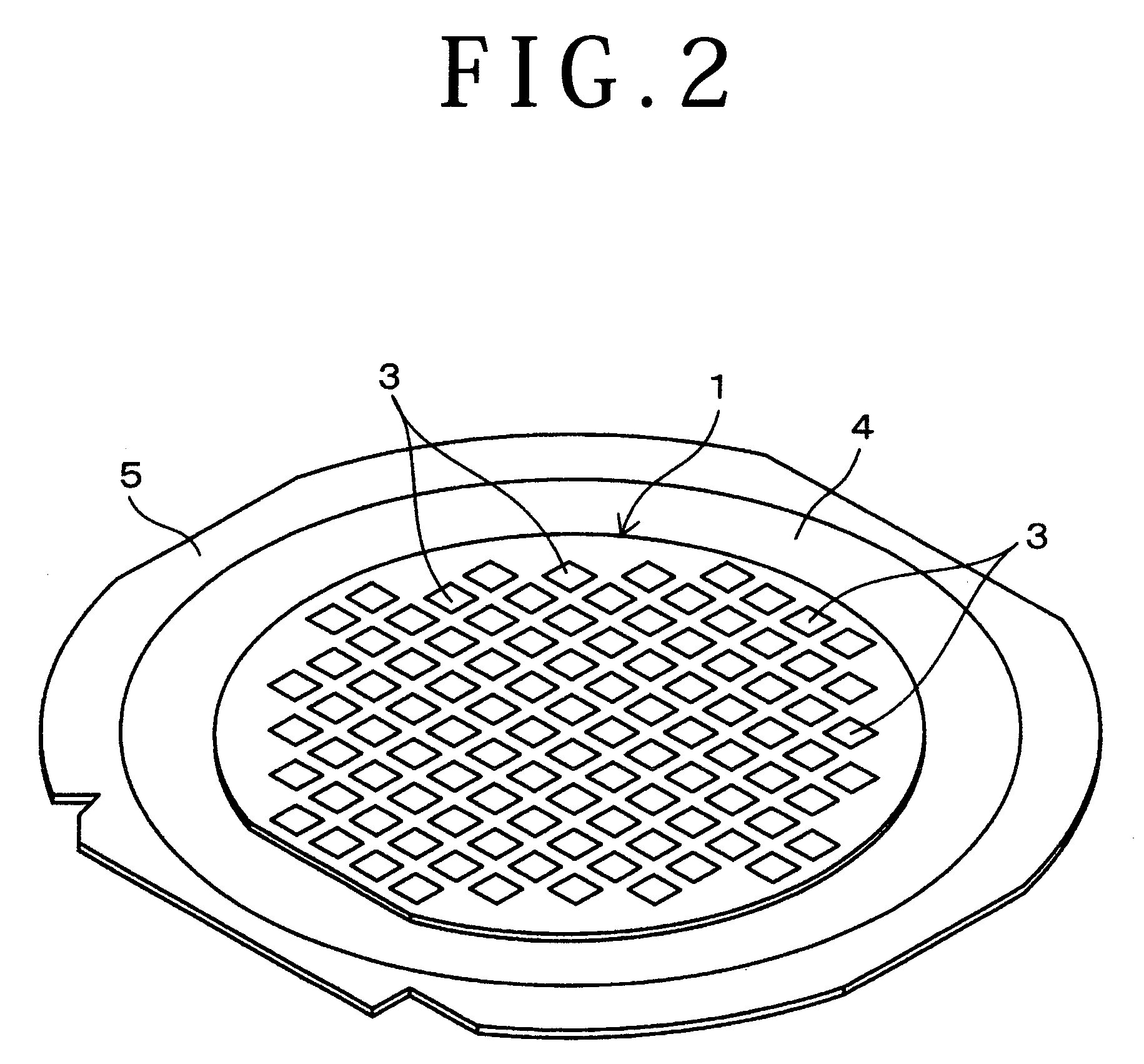
[0026][1] Workpiece (Semiconductor Wafer)

[0027]FIG. 1 shows a workpiece like a thin sheet as an object to be processed according to this preferred embodiment. This workpiece is a disk-shaped semiconductor wafer (which will be hereinafter referred to simply as wafer) such as a silicon wafer. For example, the wafer 1 has a thickness of about 200 μm and a diameter of about 200 mm. The outer circumferential portion of the wafer 1 is partially cut off to form an orientation flat 2 as a mark for indicating a crystal orientation.

[0028]The front side of the wafer 1 is formed with a plurality of first streets A extending in a first direction (horizontal direction as viewed in FIG. 1) and a plurality of second streets B extending in a second direction (vertical direction as viewed in FIG. 1) perpendicular to the first direction. The first streets A extend parallel to each other at equal ...


PUM

PropertyMeasurementUnit
diameteraaaaaaaaaa
thicknessaaaaaaaaaa
thicknessaaaaaaaaaa

Abstract

A laser processing method including a first step of forming a first groove and a second step of forming a second groove on the workpiece. In the first step, the laser beam is intermittently applied to the first street except the intersections between the first street and the second street, thereby forming a discontinuous groove as the first groove in such a manner that each intersection is not grooved. In the second step, the laser beam is continuously applied to the second street, thereby forming a continuous groove as the second groove intersecting the first groove in such a manner that each intersection is grooved by the second groove. In the second step, heat generated at a portion immediately before each intersection is passed through the intersection to be dissipated forward, thereby suppressing overheating at this portion.

Description

BACKGROUND OF THE INVENTION[0001]1. Field of the Invention[0002]The present invention relates to a laser processing method for forming a plurality of grooves in relation to a thin platelike workpiece such as a semiconductor wafer by applying a laser beam, and more particularly to a laser processing method suitable in the case that the grooves intersect each other.[0003]2. Description of the Related Art[0004]In a fabrication process for semiconductor devices (chips), a plurality of rectangular chip areas are partitioned by a plurality of crossing streets (division lines) formed on the front side of a substantially disk-shaped semiconductor wafer, and an electronic circuit such as IC or LSI is formed in each chip area. Thereafter, the back side of the wafer is ground as required and the wafer is next cut to be divided along all of the streets (dicing step) to obtain the individual chip areas as semiconductor chips. Each semiconductor chip thus obtained is packaged with a sealing resin...

Claims


Application Information

Patent Timeline
Patent Type & Authority Applications(United States)
IPC IPC(8): H01L21/78B23K26/38B23K26/364B28D5/00
CPCB23K26/0853H01L21/78B23K26/4075B23K26/367B23K26/364B23K26/40B23K2103/50
Inventor MORIKAZU, HIROSHIUEMURA, SHINICHIRO
Owner DISCO CORP
Why Eureka
Try Eureka