Single event transient mitigation and measurement in integrated circuits

a single-event transient and integrated circuit technology, applied in the field of integrated circuits, can solve the problems of volatile control elements such as sram bits, unsuitable or unreliable for a variety of uses, loss of programming data,

Active Publication Date: 2009-08-13
MICROSEMI SOC
View PDF21 Cites 248 Cited by
  • Summary
  • Abstract
  • Description
  • Claims
  • Application Information

AI Technical Summary

Problems solved by technology

It is also well known in the art that CMOS integrated circuits are vulnerable to a variety of radiation effects that make them unsuitable or unreliable for a variety of uses in the aerospace, space, and military fields without a degree of radiation hardening appropriate for the particular radiation environment anticipated for the application.
Unfortunately, this typically requires drivers to be far larger than the minimum or near-minimum sized transistors that are desirable to use in logic circuits.
Volatile control elements, such as SRAM bits, lose their programming data when the PLD power supply is disconnected, disabled or turned off.

Method used


Image

  • Single event transient mitigation and measurement in integrated circuits
  • Single event transient mitigation and measurement in integrated circuits
  • Single event transient mitigation and measurement in integrated circuits

Examples


Embodiment Construction

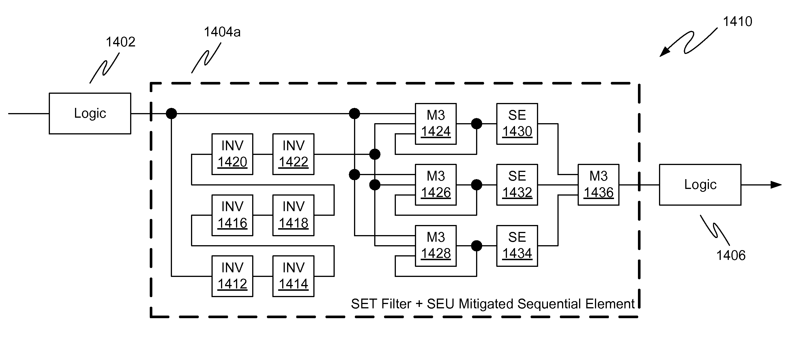
[0064]Persons of ordinary skill in the art will realize that the following description of the present invention is illustrative only and not in any way limiting. Other embodiments of the invention will readily suggest themselves to such skilled persons.

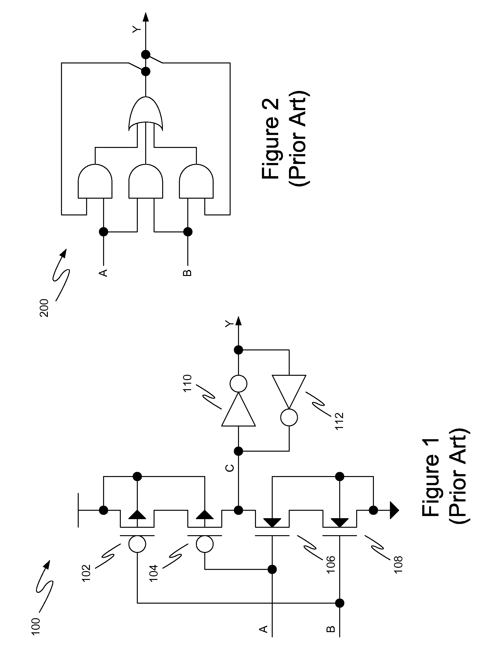
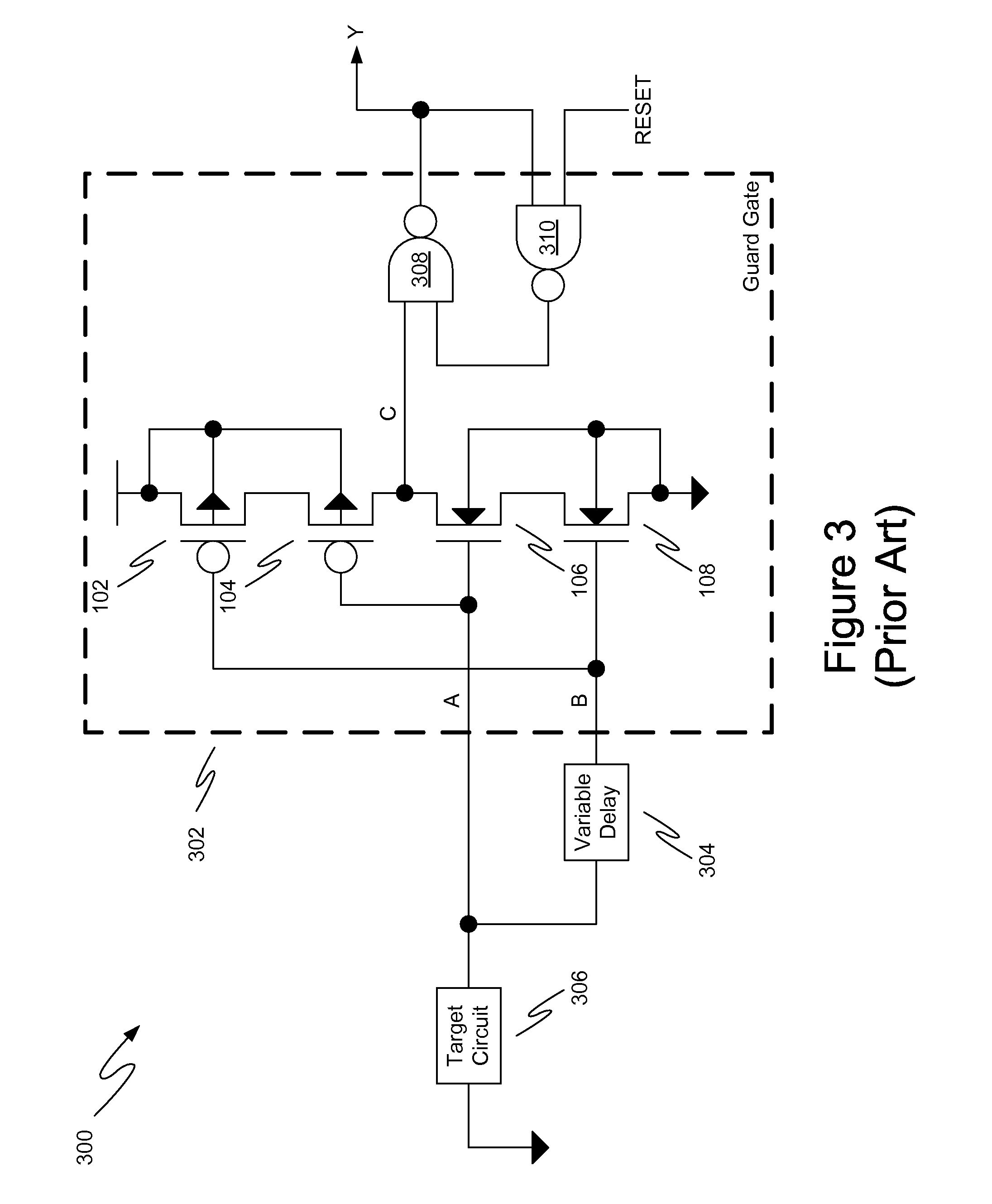
[0065]For purposes of this specification, nominally equivalent logic signals are output signals from different circuits each implementing the same Boolean function of the same input variables. The input variables to the different circuits need not be the same exact set of input signals, if the input variables themselves are present as sets of nominally equivalent logic signals. Two nominally equivalent logic signals would always have the same value in an ideal static situation like, for example, if the input variables never change and there is no radiation present. In normal operation, nominally equivalent logic signals may have different values for short periods of time due to logic transitions and particle strikes. Two nominally equ...


PUM


Abstract

A method for single event transient filtering in an integrated circuit device is described. The device comprises three sequential elements, each having a data input and a data output with each of the three data outputs coupled to one of three inputs of a voting gate. The method comprises generating first and second nominally equivalent logic signals in first and second SET domains, converting the first and second nominally equivalent logic signals into first, second and third nominally equivalent data channels, and transmitting the first, second and third nominally equivalent data channels to the data inputs of the first, second and third sequential elements. Provision is made for applying the method to logic designs implemented in programmable logic integrated circuit devices.

Description

REFERENCE TO RELATED APPLICATIONS[0001]This application is a continuation in part of application Ser. No. 12 / 352,512 filed Jan. 12, 2009, which claims benefit under 35 USC §119(e) from Provisional Application No. 61 / 024,146 filed Jan. 28, 2008, both of which are hereby incorporated herein by reference.BACKGROUND OF THE INVENTION[0002]1. Field of the Invention[0003]The invention pertains to the field of integrated circuits. More particularly, the invention pertains to radiation hardening of integrated circuit devices.[0004]2. The Prior Art[0005]CMOS integrated circuits are well known in the art and are used in thousands of different applications. It is also well known in the art that CMOS integrated circuits are vulnerable to a variety of radiation effects that make them unsuitable or unreliable for a variety of uses in the aerospace, space, and military fields without a degree of radiation hardening appropriate for the particular radiation environment anticipated for the application...

Claims


Application Information

Patent Timeline
Patent Type & Authority Applications(United States)
IPC IPC(8): G06F17/50
CPCH03K19/0033
Inventor REZGUI, SANA
Owner MICROSEMI SOC
Why Eureka
Try Eureka