Method and device for reducing crosstalk in back illuminated imagers

a back illuminated imager and crosstalk technology, applied in the field of imagers, can solve the problems of significant performance limitations of front-illuminated imagers low fill factor/low sensitivity, etc., and achieve the effect of reducing crosstalk

Active Publication Date: 2009-08-20
SRI INTERNATIONAL
View PDF9 Cites 36 Cited by
  • Summary
  • Abstract
  • Description
  • Claims
  • Application Information

AI Technical Summary

Problems solved by technology

Front-illuminated imagers, however, have significant performance limitations such as low fill factor / low sensitivity.
The problem of low fill factor / low sensitivity is typically due to shadowing caused by the presence of opaque metal bus lines, and absorption by an array circuitry structure formed on the front surface in the pixel region of a front-illuminated imager.
One challenge is the loss of charge carriers near the back surface due to inherent dangling bonds present at the silicon back surface, which reduces Quantum Efficiency (QE) if the backside of the thinned imager is not pinned.
Eliminating this problem requires additional treatment at the backside of the device, which adds to the complexity of the fabrication process.
A second challenge is absorption of charge carriers within the epitaxial layer, which prevents charge carriers from reaching processing components on the front side, which reduces sensitivity and efficiency of the device.
Additional challenges include excessive thinning of wafers, which poses yield issues such as stress in the thinned wafer, and uniformity of thickness, etc.
Fabrication cost of back illuminated imagers can be higher than for front illuminated imagers due to thinning and backside treatment.
However, as technology advances in the fabrication of CMOS devices, the current CMOS imaging market demands high pixel density, and hence small pixel size for imagers.
This limits the drift field that can be produced in a small pixel back illuminated imager array.

Method used


Image

  • Method and device for reducing crosstalk in back illuminated imagers
  • Method and device for reducing crosstalk in back illuminated imagers
  • Method and device for reducing crosstalk in back illuminated imagers

Examples


embodiment-1

Method Use of Higher Energy Implants to Create Electrical Barriers

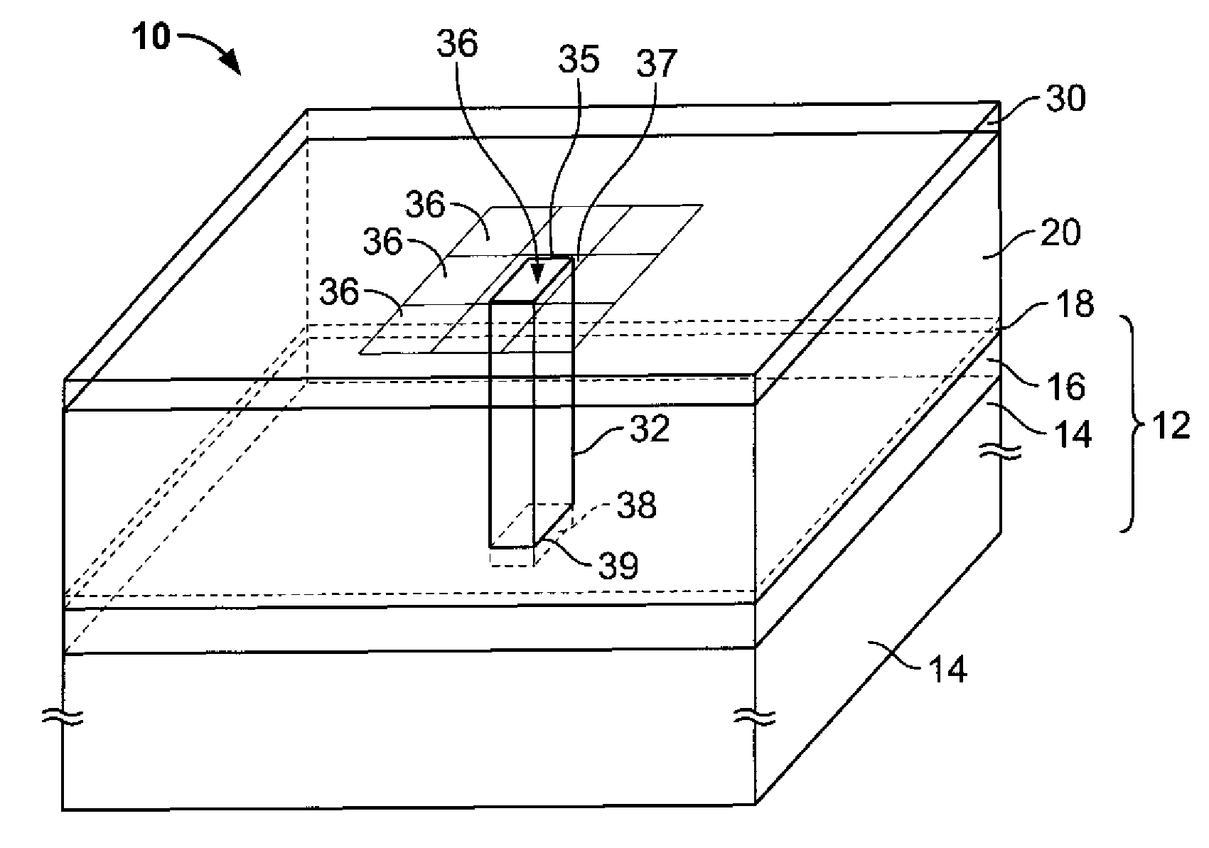
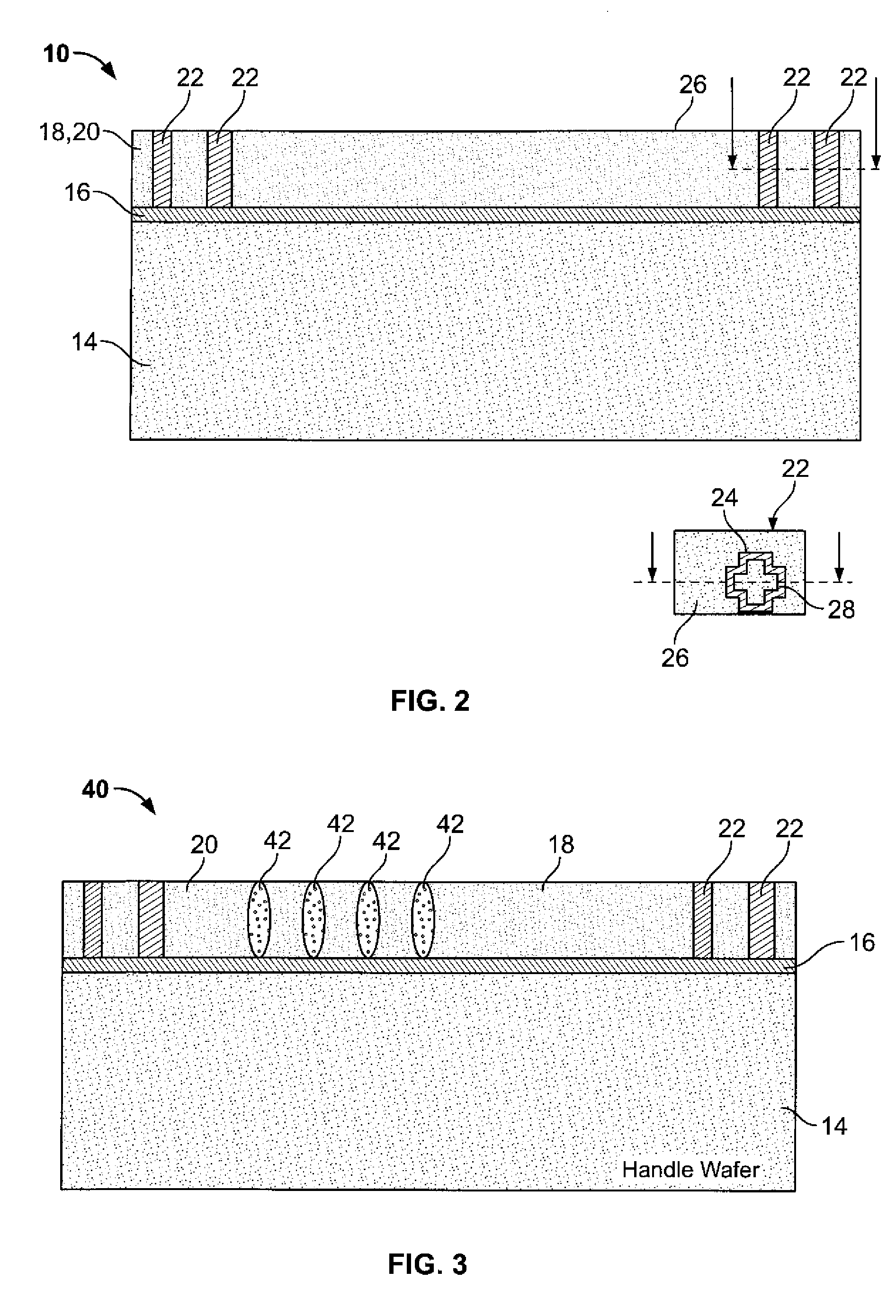
[0038]FIG. 3 shows a cross-section of an imager 40 having a plurality of isolation barriers formed therein by means of implanted dopants. The high-energy implants 42 are formed from available techniques in the fabrication industry. Today's high-energy (on the order of MeV) implanters are capable of implanting species in the range of 2-10 um deep into silicon. Referring now to FIGS. 1-4, a method 50 for forming isolation barriers made from high energy implants is described as follows:

[0039]At step 52, an SOI wafer 12 which has a thin Si seed layer 18 is provided. At step 54, an epitaxial layer 20 with a desired thickness (2-10 um) and resistivity is grown on the seed layer 18. At step 55, the doping profile of the epitaxial layer 20 is engineered according to the technique described in the '583 Patent. At step 56, alignment keys 22 are formed in the epitaxial layer 20. Sub-steps include printing alignment keys on the ...

embodiment-2

Method Use of Oxide Trenches to Create Electrical Barriers

[0040]FIG. 5 shows a cross-section of an imager 64 having a plurality of isolation barriers formed therein by means of oxide trenches. The oxide trenches 66, being insulators, act as electrical barriers to generated charge carriers and confine them within pixel collecting wells. One advantage of this method is that the barrier trenches 66 can be defined along with the alignment keys, eliminating the need for another photo mask. Referring now to FIGS. 1-2, 5 and 6, a method 68 for forming isolation barriers made from oxide trenches is described as follows:

[0041]At step 70, an SOI wafer 12 which has a thin Si seed layer 18 is provided. At step 72, an epitaxial layer 20 with a desired thickness (2-10 um) and resistivity is grown on the seed layer 18. At step 73, the doping profile of the epitaxial layer 20 is engineered according to the technique described in the '583 Patent. At step 74, trench outlines are formed about collect...

embodiment-3

Method Use of both Higher Energy Implants and Oxide Trenches to Create Electrical Barriers:

[0043]FIG. 7 shows a cross-sectional of all imager 84 having a plurality of isolation barriers 86 formed therein by means of both oxide trenches 88 and high energy implants 90, thereby combining methods 1 and 2 by creating oxide trenches and implanting dopants around those trenches. Referring now to FIGS. 1-2 and 7 and 8, a method 92 for forming isolation barriers made from oxide trenches and high energy implants is described as follows:

[0044]The method 92 begins by performing steps 70 to 80 of the method 68 to create oxide trenches and alignment keys. At step 94, regions about each of the filled trenches are opened down to the oxide layer 18, and at step 96, the regions are implanted with high energy dopants, the dopants being thermally activated thereupon. At step 97, imaging structures 30 are formed overlying the epitaxial layer 20. Since the oxide trenches are encapsulated by dopants, the...


PUM


Abstract

A method and resulting device for reducing crosstalk in a back-illuminated imager is disclosed, comprising providing a substrate comprising an insulator layer and a seed layer substantially overlying the insulator layer, an interface being formed where the seed layer comes in contact with the insulator layer; forming an epitaxial layer substantially overlying the seed layer, the epitaxial layer defining plurality of pixel regions, each pixel region outlining a collection well for collecting charge carriers; and forming one of an electrical, optical, and electrical and optical barrier about the outlined collection well extending into the epitaxial layer to the interface between the seed layer and the insulator layer. The seed layer and the epitaxial layer of the device have a net dopant concentration profile which has an initial maximum value at the interface of the seed layer and the insulator layer and which decreases monotonically with increasing distance from an interface within an initial portion of the semiconductor substrate and the epitaxial layer.

Description

CROSS-REFERENCE TO RELATED APPLICATIONS[0001]This application claims the benefit of U.S. provisional patent application No. 61 / 029,648 filed Feb. 19, 2008, the disclosure of which is incorporated herein by reference in its entirety.FIELD OF THE INVENTION[0002]The present invention relates generally to imagers, and more particularly, to a method and resulting device for reducing crosstalk in back illuminated imagers.BACKGROUND OF THE INVENTION[0003]CMOS or CCD image sensors are of interest in a wide variety of sensing and imaging applications in a wide range of fields including consumer, commercial, industrial, and space electronics. Imagers based on charge coupled devices (CCDs) are currently the most widely utilized. CCDs are employed either in front or back illuminated configurations. Front illuminated CCD imagers are more cost effective to manufacture than back illuminated CCD imagers such that front illuminated devices dominate the consumer imaging market. Front-illuminated imag...

Claims


Application Information

Patent Timeline
Patent Type & Authority Applications(United States)
IPC IPC(8): H01L31/00H01L21/00
CPCH01L27/1463H01L27/1464H01L27/14689H01L27/14687
Inventor SWAIN, PRADYUMNA KUMARBHASKARAN, MAHALINGAM
Owner SRI INTERNATIONAL
Why Eureka
Try Eureka