
Emulation of abstracted DIMMs using abstracted DRAMs

a technology of abstracted dimms and drams, applied in the field of semiconductor memory, can solve problems such as non-optimal memory subsystems and performance reduction, and achieve the effect of memory performan

Active Publication Date: 2009-08-27
GOOGLE LLC
View PDF99 Cites 88 Cited by
  • Summary
  • Abstract
  • Description
  • Claims
  • Application Information

AI Technical Summary

Benefits of technology

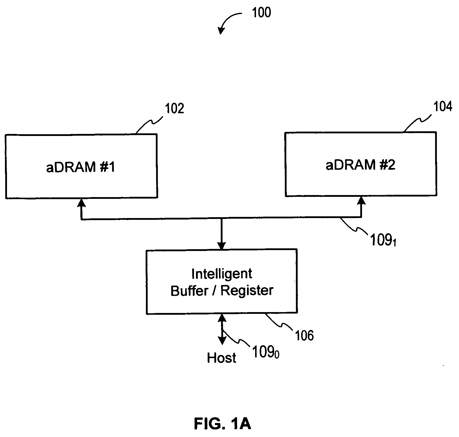
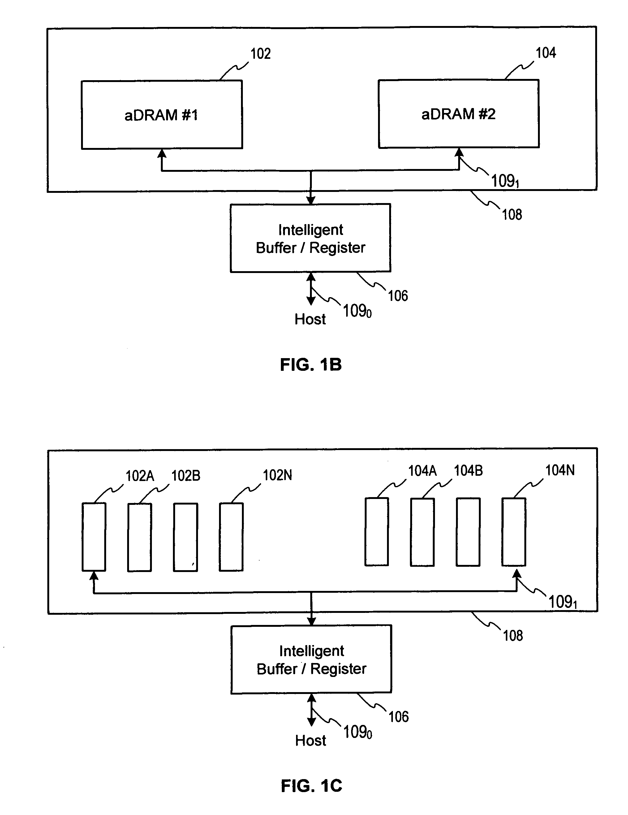
[0006]The present invention sets forth an abstracted memory subsystem comprising abstracted memories, which each may be configured to present memory-related characteristics onto a memory system interface. The characteristics can be presented on the memory system interface via logic signals or protocol exchanges, and the characteristics may include any one or more of, an address space, a protocol, a memory type, a power management rule, a number of pipeline stages, a number of banks, a mapping to physical banks, a number of ranks, a timing characteristic, an address decoding option, a bus turnaround time parameter, an additional signal assertion, a sub-rank, a number of planes, or other memory-related characteristics. Some embodiments include an intelligent register device and / or, an intelligent buffer device. One advantage of the disclosed subsystem is that memory performance may be optimized regardless of the specific protocols used by the underlying memory hardware devices.

Problems solved by technology

The limitations imposed by memory protocols, traditional memory subsystem architectures, standards, processor-specific memory access models, end-user configurability requirements, power constraints, or combinations of those limitations tend to interact in such a manner that reduce performance and result in non-optimal memory subsystems.

Method used


Image

  • Emulation of abstracted DIMMs using abstracted DRAMs
  • Emulation of abstracted DIMMs using abstracted DRAMs
  • Emulation of abstracted DIMMs using abstracted DRAMs

Examples


embodiment 200

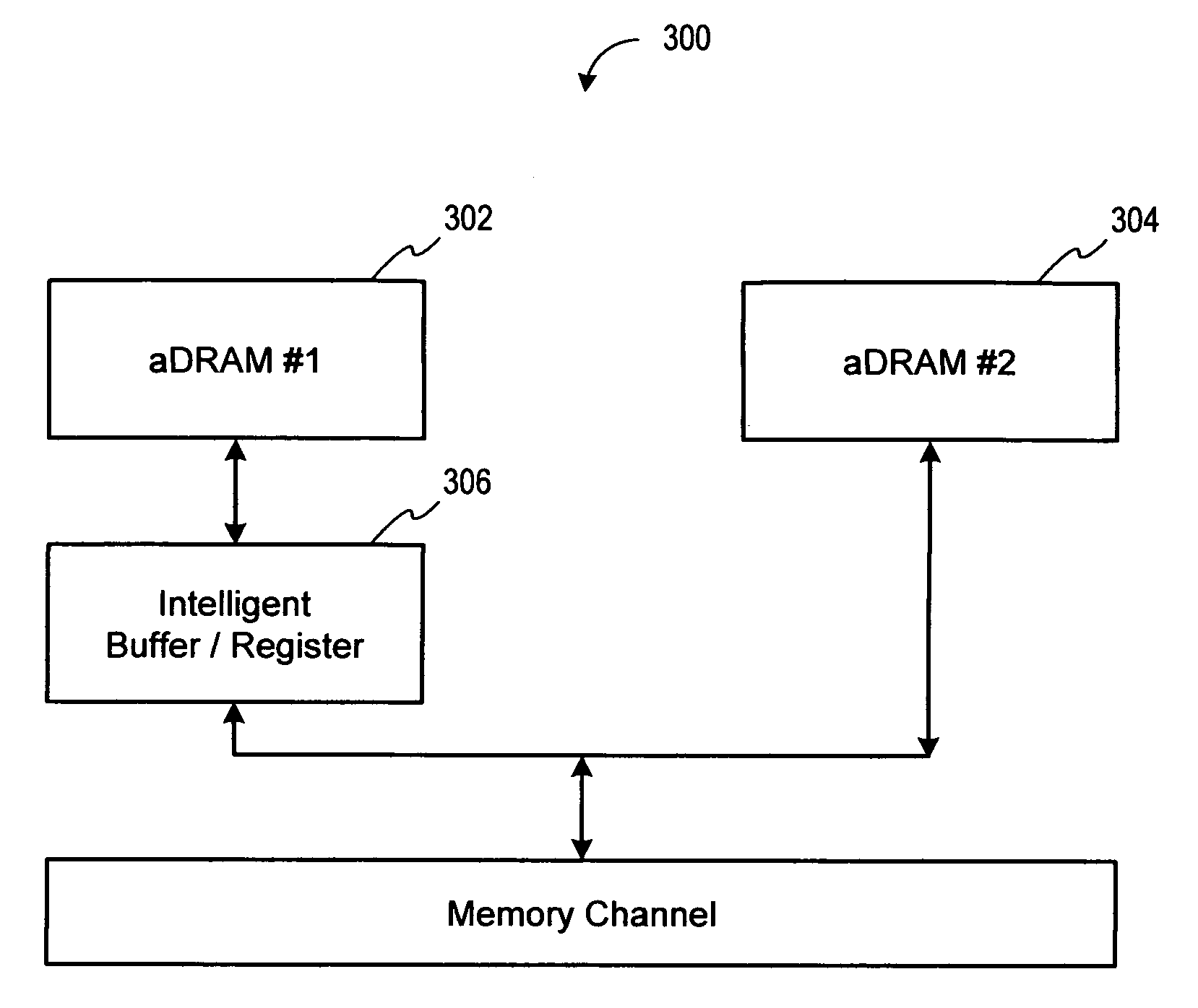
[0043]In embodiment 200, illustrated in FIG. 2, two independently controlled address spaces may be implemented using an identical type of physical memory. In other embodiments, the two independently controlled address spaces may be implemented with each using a different type of physical memory.

[0044]In other embodiments, the size of the address space of the memory under conservative management 202 is programmable, and applied to the address space at appropriate times, and is controlled by the intelligent register in response to commands from a host (not shown). The address space of the memory at 204 is similarly controlled to implement a different power management regime.

[0045]The intelligent buffer can present to the memory controller a plurality of timing parameter options, and depending on the specific selection of timing parameters, engage more aggressive power management features as described.

Abstracted DRAM Having Adjustable Timing Characteristics

[0046]In the embodiment just ...

third embodiment

[0049]In a third embodiment capable of presenting different aDRAM timing characteristics, the intelligent buffer may present to the controller different options for tWL, the write-latency timing parameter. Depending on the amount of latency added to tWL, the intelligent buffer may be able to lower the clock-enable signal to one or more sets of memory devices. (e.g. to deploy CKE-after-write, or not to deploy it, depending on tWL).

Changing Configurations to Enable / Disable Aggressive Power Management

[0050]Different memory (e.g. DRAM) circuits using different standards or technologies may provide external control inputs for power management. In DDR2 SDRAM, for example, power management may be initiated using the CKE and CS inputs and optionally in combination with a command to place the DDR2 SDRAM in various powerdown modes. Four power saving modes for DDR2 SDRAM may be utilized, in accordance with various different embodiments (or even in combination, in other embodiments). In particu...


PUM


Abstract

One embodiment of the present invention sets forth an abstracted memory subsystem comprising abstracted memories, which each may be configured to present memory-related characteristics onto a memory system interface. The characteristics can be presented on the memory system interface via logic signals or protocol exchanges, and the characteristics may include any one or more of, an address space, a protocol, a memory type, a power management rule, a number of pipeline stages, a number of banks, a mapping to physical banks, a number of ranks, a timing characteristic, an address decoding option, a bus turnaround time parameter, an additional signal assertion, a sub-rank, a number of planes, or other memory-related characteristics. Some embodiments include an intelligent register device and / or, an intelligent buffer device. One advantage of the disclosed subsystem is that memory performance may be optimized regardless of the specific protocols used by the underlying memory hardware devices.

Description

CROSS REFERENCE TO RELATED APPLICATIONS[0001]This application claims the priority benefit of U.S. Provisional Patent Application No. 61 / 030,534, filed on Feb. 21, 2008. The subject matter of the above related application is hereby incorporated herein by reference, however, insofar as any definitions, information used for claim interpretation, etc. from the above parent application conflict with that set forth herein, such definitions, information, etc. in the present application should apply.FIELD OF THE INVENTION[0002]The present invention relates to semiconductor memory and more particularly to memory subsystems used in computing platforms.BACKGROUND[0003]Conventional memory systems typically consist of one or more memory devices, such as dynamic random access memories (e.g. DRAMs), mounted on a Printed Circuit Board (PCB) called a Dual In-line Memory Module (DIMM). The memory system is in communication with a memory controller (MC) which in turn is in communication with a process...

Claims


Application Information

Patent Timeline
Patent Type & Authority Applications(United States)
IPC IPC(8): G06F12/06
CPCG06F13/4239Y02B60/1235Y02B60/1228Y02D10/00
Inventor SMITH, MICHAEL J.S.RAJAN, SURESH NATARAJANWANG, DAVID T.
Owner GOOGLE LLC
Learn More