

Active device array substrate and fabrication method thereof
- Summary
- Abstract
- Description
- Claims
- Application Information
AI Technical Summary
Benefits of technology
Problems solved by technology
Method used
Image

Examples
first embodiment
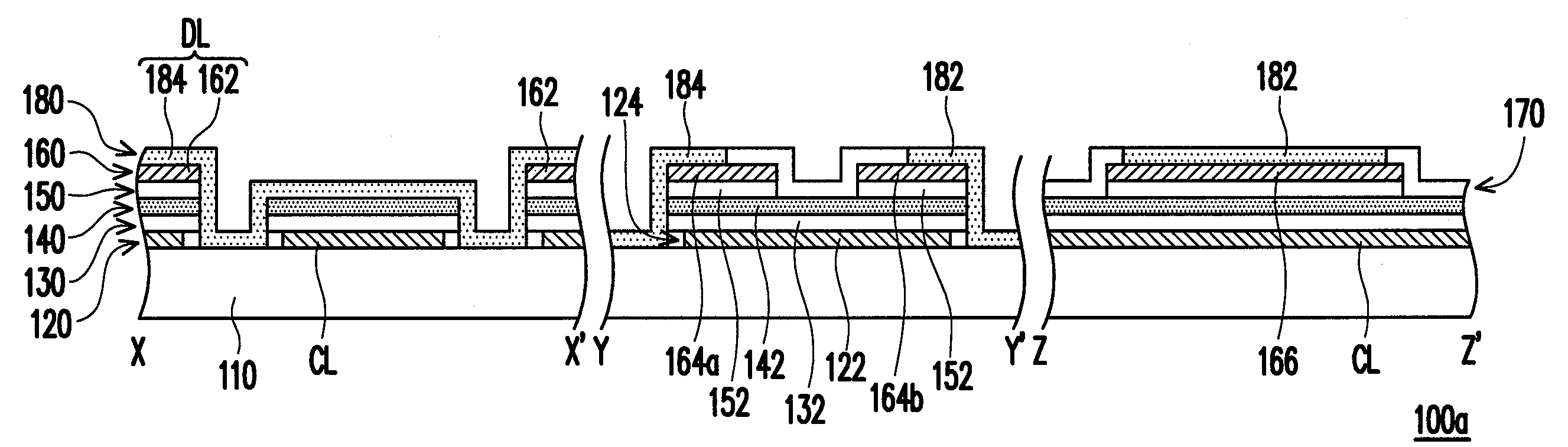
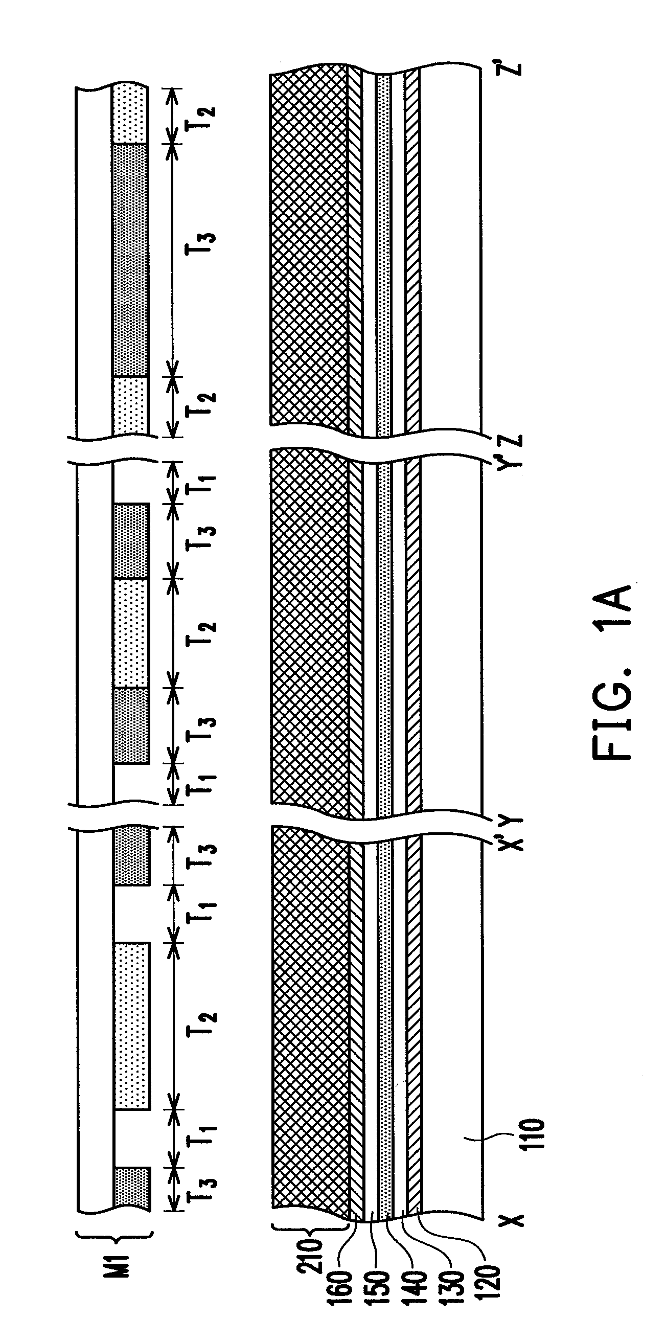
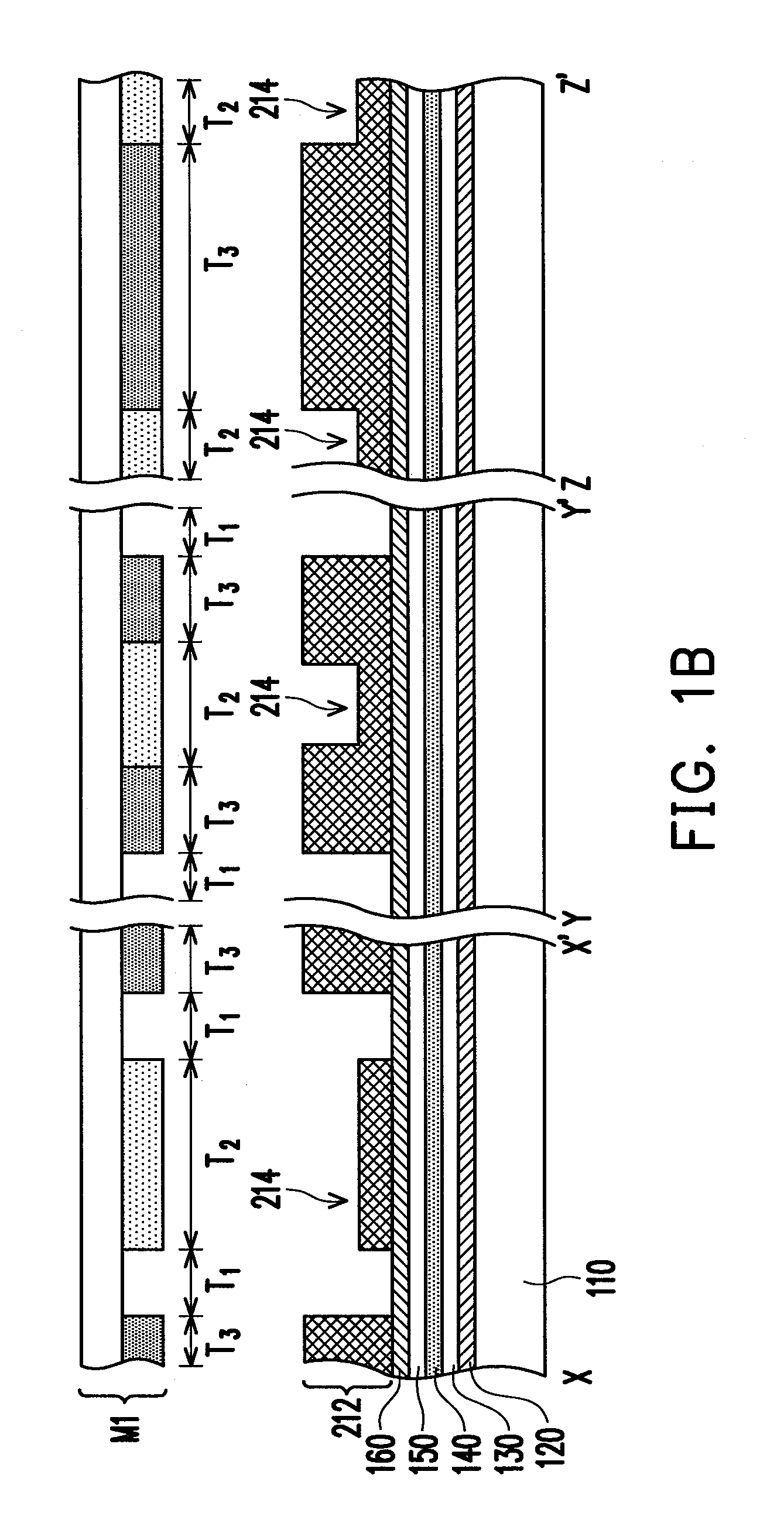
[0043]FIGS. 1A˜1H are cross-sectional views illustrating a fabrication method of an active device array substrate according to a first embodiment of the present invention, and FIGS. 2A˜2B are partial top views illustrating the fabrication method of the active device array substrate according to the first embodiment of the present invention. Referring to FIG. 1A, first, a substrate 110 is provided. Next, a first metal material layer 120, a gate insulation material layer 130, a channel material layer 140, a second metal material layer 160, and a first photoresist layer 210 are sequentially formed on the substrate 110.
[0044]More specifically, the first metal material layer 120 may be formed by depositing a metal material on the substrate 110 through physical vapor deposition (PVD), and the material thereof may be of a low resistance material, such as Al, Au, Cu, Mo, Cr, Ti, Al alloy, or Mo alloy. The gate insulation material layer 130 may be deposited on the first metal material layer ...
PUM
 Abstract
Description
Claims
Application Information