
Light modulating device

a light modulating device and light technology, applied in the field of light modulating devices, can solve the problems of low absolute value of chirp amount, degraded manufacturing yield, and high modulation voltage, and achieve stable implementation, satisfactory reproducibility, and stable long distance transmission

Inactive Publication Date: 2009-09-03
LAPIS SEMICON CO LTD
View PDF6 Cites 7 Cited by
  • Summary
  • Abstract
  • Description
  • Claims
  • Application Information

AI Technical Summary

Benefits of technology

[0011]The present invention has been made in view of the foregoing points. It is an object of the present invention to provide a Mach-Zehnder type modulating device (MZ modulating device or modulator) which is easy to fabricate and capable of stably obtaining a desired negative chirp characteristic suitable for long distance transmission. It is also an object of the present invention to provide an MZ modulating device which can be operated with both of a negative chirp characteristic and a zero chirp characteristic by a single device.
[0013]According to the present invention, the thicknesses of the core layers of the two waveguides that perform the optical phase modulation in the MZ light modulator are made different from each other thereby to bring the configurations of the two waveguides that perform the corresponding modulation into asymmetry. The relationship between the magnitudes of the modulation voltages (center voltages) for the two modulation waveguides is changed thereby to enable implementation of both of a negative chirp operation and a zero chirp operation. Thus, a light modulating device can be provided wherein a modulation condition is changed by a single device thereby to make it possible to implement both negative chirp and zero chirp, thus enabling flexible adaptation to various different demands of a system.
[0014]Further, the negative chirp characteristic and the zero chirp characteristic can be implemented stably and with satisfactory reproducibility. Along with it, long distance transmission can be realized stabler without incurring a reduction in extinction ratio.

Problems solved by technology

Since, however, only one arm waveguide is driven to perform the light modulation, a high modulation voltage is required.
The conventional push-pull drive was accompanied by a problem that the absolute value of a chirp amount was small even if the negative chirp characteristic could be obtained.
The above related art had however a problem that great unequal division of the branching ratio with satisfactory reproducibility (4:6, 3:7 and the like) was very difficult and the manufacturing yield was degraded.
A problem also arose in that since an extinction ratio was reduced where the branching ratio was shifted from 1:1, the identification of post-transmission On / Off became difficult correspondingly.
Further, a problem arose in that there was a need to make a modulation voltage higher for the purpose of obtaining an extinction ratio necessary for high-speed and long distance transmission.

Method used


Image

  • Light modulating device
  • Light modulating device
  • Light modulating device

Examples


first preferred embodiment

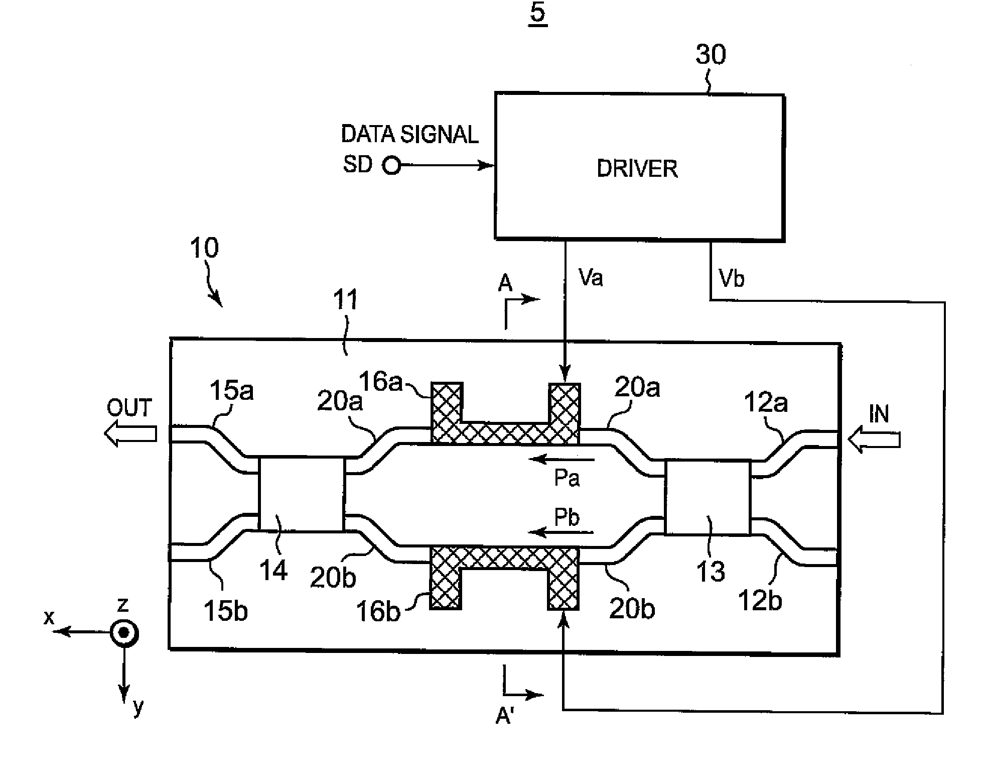
[0023]FIG. 1 is a diagram showing a configuration of a light modulating device 5 illustrative of a first embodiment of the present invention. The light modulating device 5 comprises a Mach-Zehnder light modulator (MZ light modulator) 10 and a driver (driver circuit) 30 of the MZ light modulator 10. A plan view of the MZ light modulator 10 is shown in FIG. 1. FIG. 2 is a sectional view taken along line A-A′ (FIG. 1) of the MZ light modulator 10.

[Configuration of Light Modulating Device]

[0024]The driver circuit 30 of the light modulating device 5 is connected to a common electrode 17 and first and second modulation electrodes 16a and 16b of the MZ light modulator 10 to be described later. The driver circuit 30 is supplied with a data signal SD. The driver circuit 30 generates modulation voltages Va and Vb, based on the received data signal SD and applies the same to the first and second modulation electrodes 16a and 16b respectively. Incidentally, the operation of the driver circuit 3...

second preferred embodiment

[0062]The above embodiment has explained the MZ light modulator wherein the thicknesses of the core layers (thicknesses of modulation layers) of the first and second arm waveguides are made asymmetric. In the present embodiment, first and second arm waveguides are identical in layer structure and core layers are set equal in thickness. However, a branching ratio of an optical demultiplexer 13 is shifted from 1, and the intensities Pa and Pb of light waveguided by the first and second arm waveguides 20a and 20b differ from each other (Pa≠Pb).

[0063]A description will hereinafter be made, as an example, of the case where the intensity (Pb) of light waveguided by the second arm waveguide 20b is larger than the intensity (Pa) of light waveguided by the first arm waveguide 20a (Pa<Pb).

[0064]Even in such a case, both negative and zero chirp operations can be realized by performing modulation in a manner similar to the first preferred embodiment. Described more specifically, a driver circui...


PUM

PropertyMeasurementUnit
thicknessaaaaaaaaaa
widthaaaaaaaaaa
electric fieldsaaaaaaaaaa

Abstract

The present invention provides an MZ light modulator that can be operated with both of a negative chirp characteristic and a zero chirp characteristic by a single device. The MZ light modulator has first and second waveguides that respectively waveguide two branched lights equal in intensity and perform optical phase modulation by application of first and second modulation voltage signals. Core layers to which modulating electric fields of the first and second waveguides are applied, are different in thickness from each other. The first and second modulation voltage signals are push-pull signals opposite in phase to each other and are different in center voltage from each other.

Description

BACKGROUND OF THE INVENTION [0001]The present invention relates to a light modulating device having a Mach-Zehnder light modulator used in optical communications and an optical information processing system or the like, and particularly to control of wavelength chirp characteristics.[0002]A Mach-Zehnder type light or optical modulator (hereinafter called also “MZ light modulator”) has been widely used as a light source of an optical communication system. The Mach-Zehnder type light modulator is of a light intensity modulator which performs On / Off of light according to an interference condition at the time that it temporarily branches or demultiplexes light into two and multiplexes the two again. The interference condition used at their multiplexion is changed by applying modulating voltages to electrodes provided on waveguides for the two demultiplexed lights.[0003]As a method for driving such a Mach-Zehnder type light modulator, there are known single arm drive for performing modul...

Claims


Application Information

Patent Timeline
Patent Type & Authority Applications(United States)
IPC IPC(8): G02F1/035
CPCB82Y20/00G02F1/0121H04B10/5053G02F1/225H04B10/25137G02F1/01708
Inventor WADA, HIROSHITERASHIMA, TOKIHIRO
Owner LAPIS SEMICON CO LTD
Learn More