[0007]Setting of the parameter is based on
trial and error in which effects are set after confirmed one by one. The setting requires high technique and is significantly inefficient. The present invention is to provide the
inspection method and the inspection tool capable of solving such a problem and of setting the parameter (hereinafter, referred to as an inspection parameter) required for detecting the defect easily.
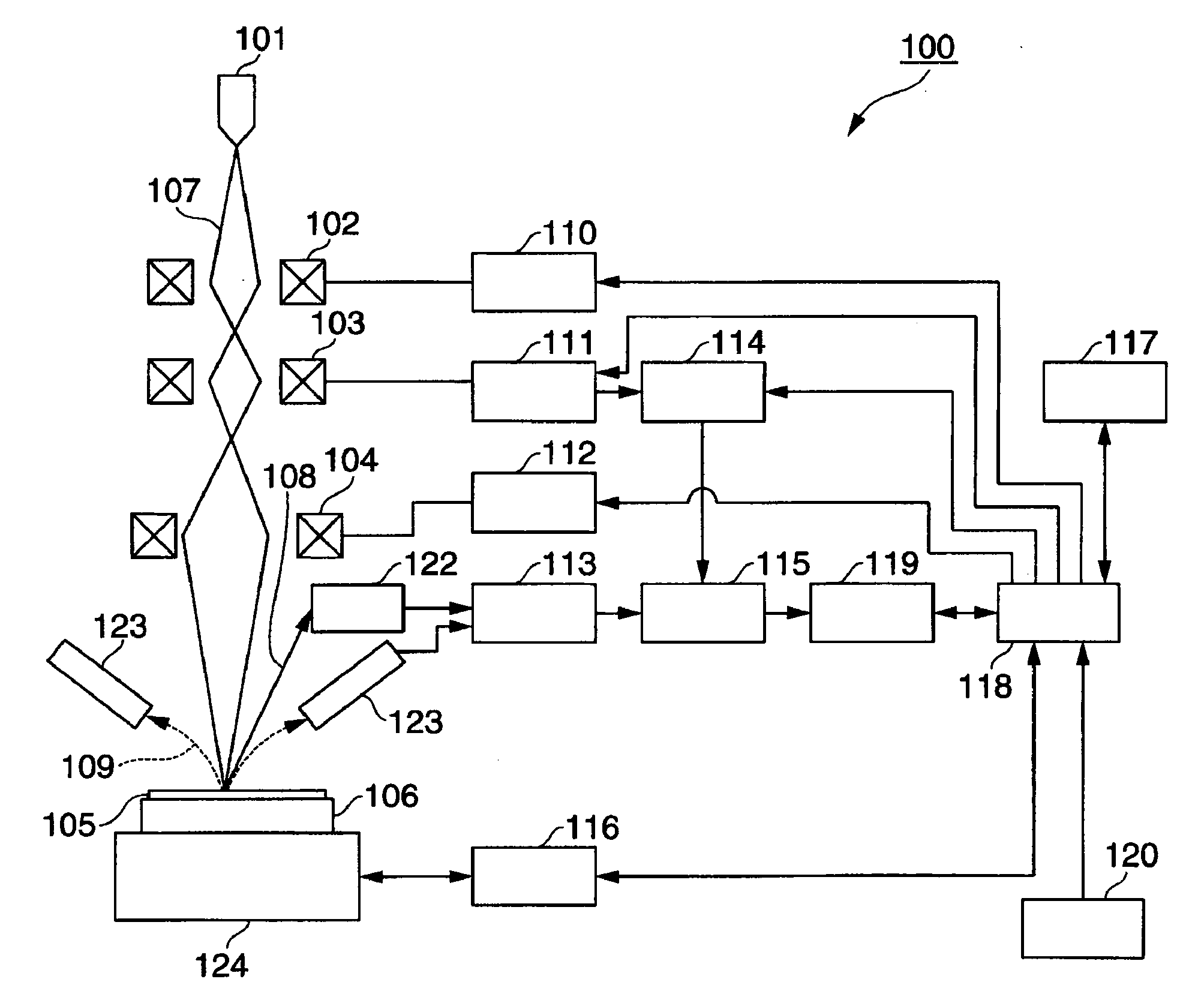
[0008]In order to solve the problem, a defect inspection tool according to the present invention comprises: an image obtaining unit for obtaining an image by applying an
electron beam to a specimen; an
image processing unit for performing a calculation process by using each predetermined inspection parameter
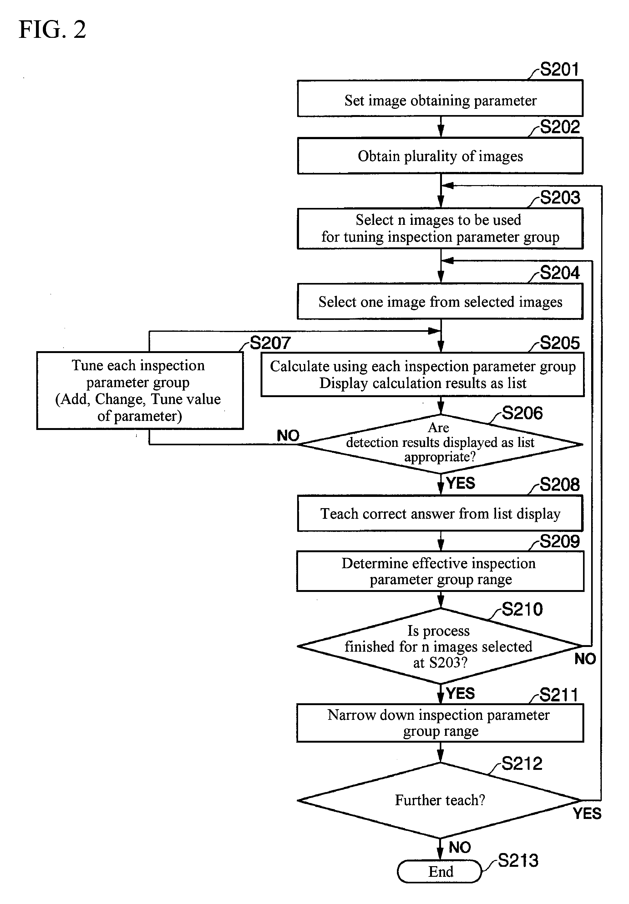
group based on the image obtained by the image obtaining unit; and a parameter tuning unit for performing a process to determine an effective inspection parameter group from calculation results by the calculation process and narrowing down an inspection parameter group range by repeating the process for a plurality of images obtained by the image obtaining unit, wherein a defect of the image obtained by the image obtaining unit is detected by using the inspection parameter group narrowed down by the parameter tuning unit. In the present invention, it becomes possible for even the user who does not understand the detailed contents of each parameter to easily tune (narrow down) complicated inspection parameter groups which are used when detecting the defect.
[0009]Also, a defect inspection tool according to another embodiment of the present invention comprises: an image obtaining unit for obtaining an image by applying an
electron beam to a specimen; an
image processing unit for performing a calculation process by using each predetermined inspection parameter
group based on the image obtained by the image obtaining unit to detect each defect detection image for each inspection parameter group; a display unit for displaying a
list of each defect detection image detected by the image
processing unit; an input unit for selectively inputting one defect detection image from each defect detection image displayed as a
list on the display unit; and a parameter tuning unit for performing a process to determine an effective inspection parameter group range from each defect detection image detected by the image
processing unit based on the defect detection image selectively inputted by the input unit and narrowing down the inspection parameter group by repeating the process for a plurality of images obtained by the image obtaining unit, wherein a defect of the image obtained by the image obtaining unit is detected by using the inspection parameter group narrowed down by the parameter tuning unit. In the present invention, it becomes possible for even the user who does not understand the detailed contents of each parameter to easily tune (narrow down) the complicated inspection parameter groups which are used when detecting the defect, by performing a simple input to select one defect detection image from each defect detection images displayed as a
list for the calculation results about a plurality of images. Meanwhile, to display the list display by the GUI allows easier selective input.
[0010]Also, a defect inspection tool according to yet another embodiment of the present invention comprises: an image obtaining unit for obtaining an image by applying an electron beam to a specimen; an image
processing unit for performing a calculation process using each predetermined inspection parameter group based on the image obtained by the image obtaining unit to detect calculation results for each inspection parameter group; an input unit for teaching a defect area included in the
image based on the image obtained by the image obtaining unit; and a parameter tuning unit for performing a process to determine an effective inspection parameter group range from the calculation results detected by the image processing unit based on the defect area taught by the input unit and narrowing down the inspection parameter group range by repeating the process for a plurality of images obtained by the image obtaining unit, wherein a defect of the image obtained by the image obtaining unit is detected by using the inspection parameter group narrowed down by the parameter tuning unit. In the present invention, it becomes possible for even the user who does not understand the detailed contents of each parameter to teach by extracting the defect area of the defect portion by the image processing by a simple input to teach the defect area of the defect portion included in the image (images by secondary electron or images by back scattered electron) displayed on the GUI, such as to draw a figure enclosing the defect portion by the input unit, to draw the defect area of the defect portion by the input unit, or to indicate the defect portion by the input unit, and to easily tune (narrow down) the complicated inspection parameter groups used when detecting the defect by performing the process for the defect portion of a plurality of images.
[0011]Meanwhile, in the present invention, it is advisable to provide various display means and functions to make the selective input and the teaching by the input unit easier, such as to provide means for synthesizing the image obtained by the image obtaining unit with each defect detection image, which is the calculation result for each inspection parameter group obtained by the calculation process by the image processing unit based on the image to display, and for simultaneously displaying the calculation result for another image, and to provide means for displaying the selected calculation result or the like in an enlarged manner. In addition, it is advisable that the display means is the GUI at that time.
[0016]The methods of tuning the inspection parameter according to the present invention allow the user who does not understand the detailed contents of each parameter to easily tune (narrow down) the complicated inspection parameter groups used when detecting the defection by the simple input, as in the case of the defect detection tool according to the present invention.

