

Threshold Voltage Consistency and Effective Width in Same-Substrate Device Groups
- Summary
- Abstract
- Description
- Claims
- Application Information
AI Technical Summary
Problems solved by technology
Method used
Image

Examples
Embodiment Construction
[0013]The making and using of the presently preferred embodiments are discussed in detail below. It should be appreciated, however, that the present invention provides many applicable inventive concepts that can be embodied in a wide variety of specific contexts. The specific embodiments discussed are merely illustrative of specific ways to make and use the invention, and do not limit the scope of the invention.
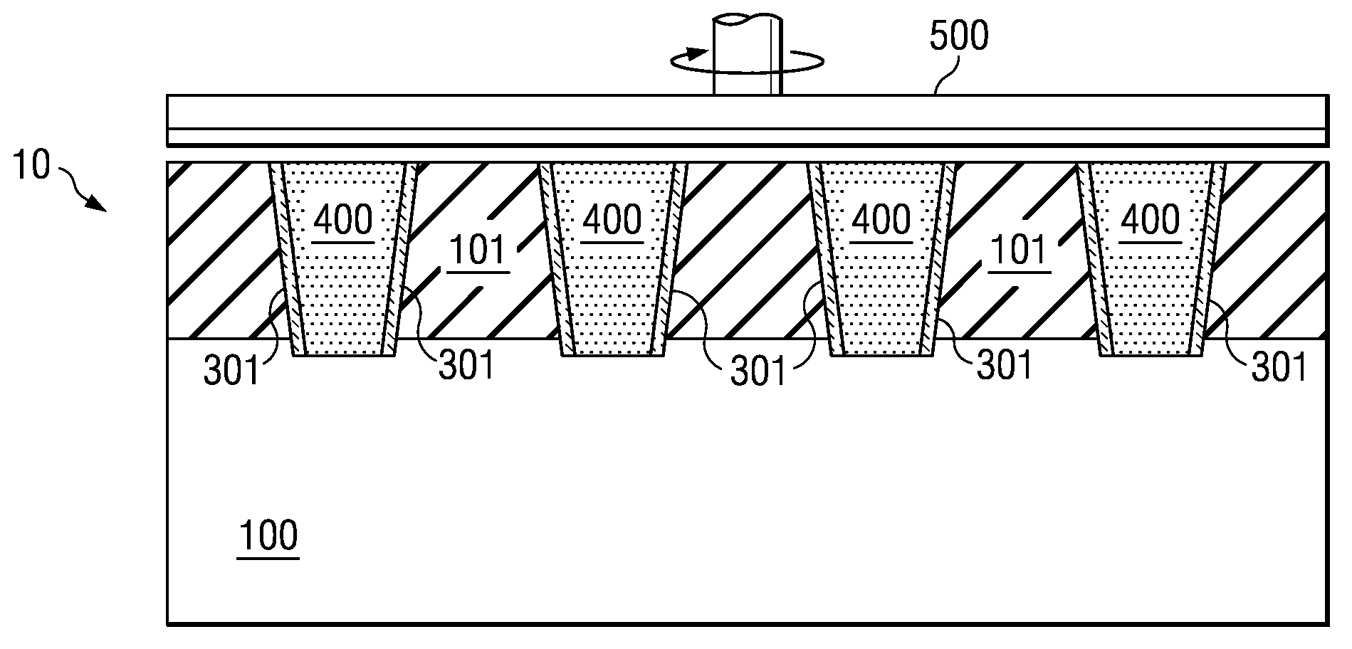
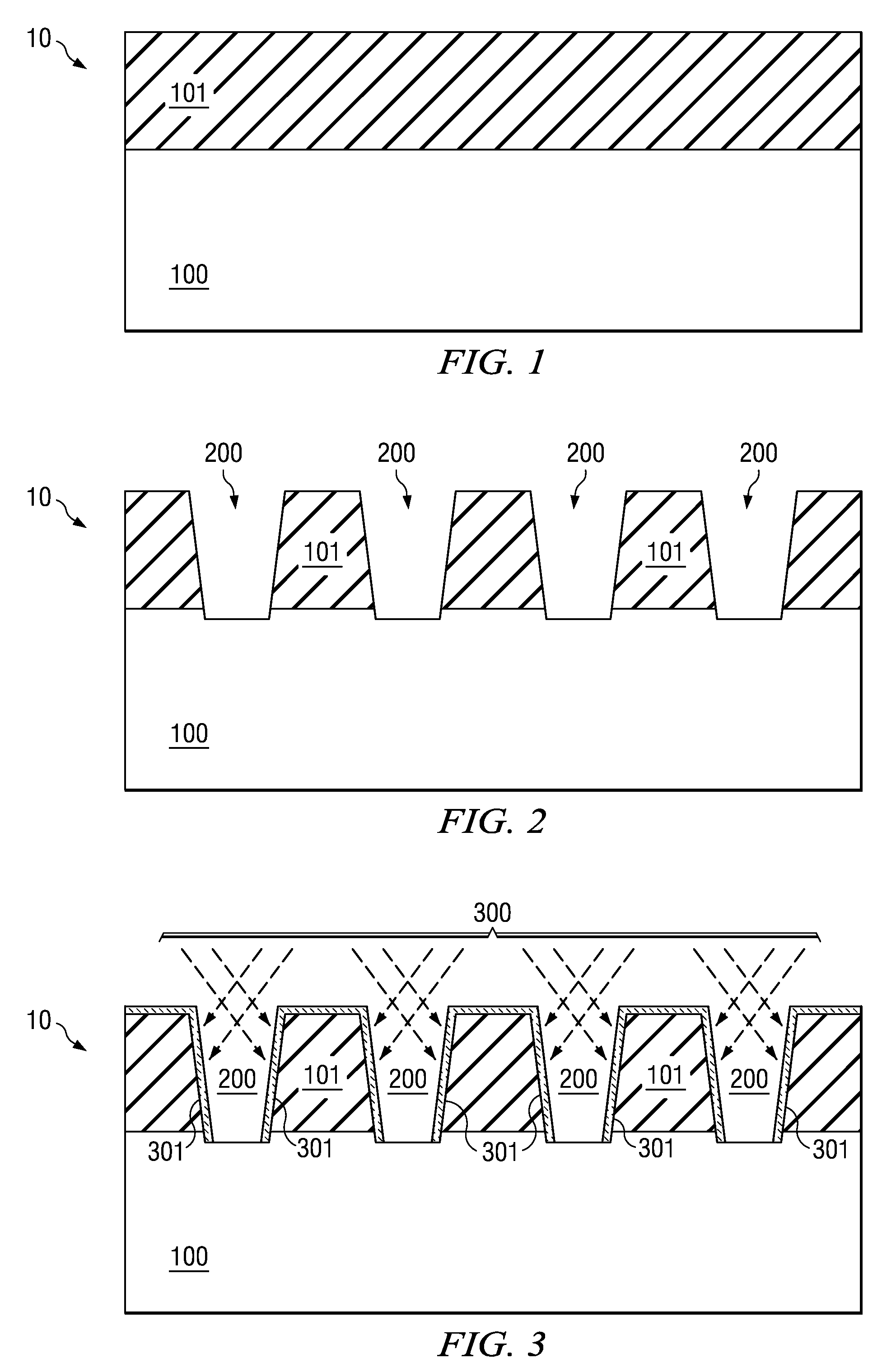
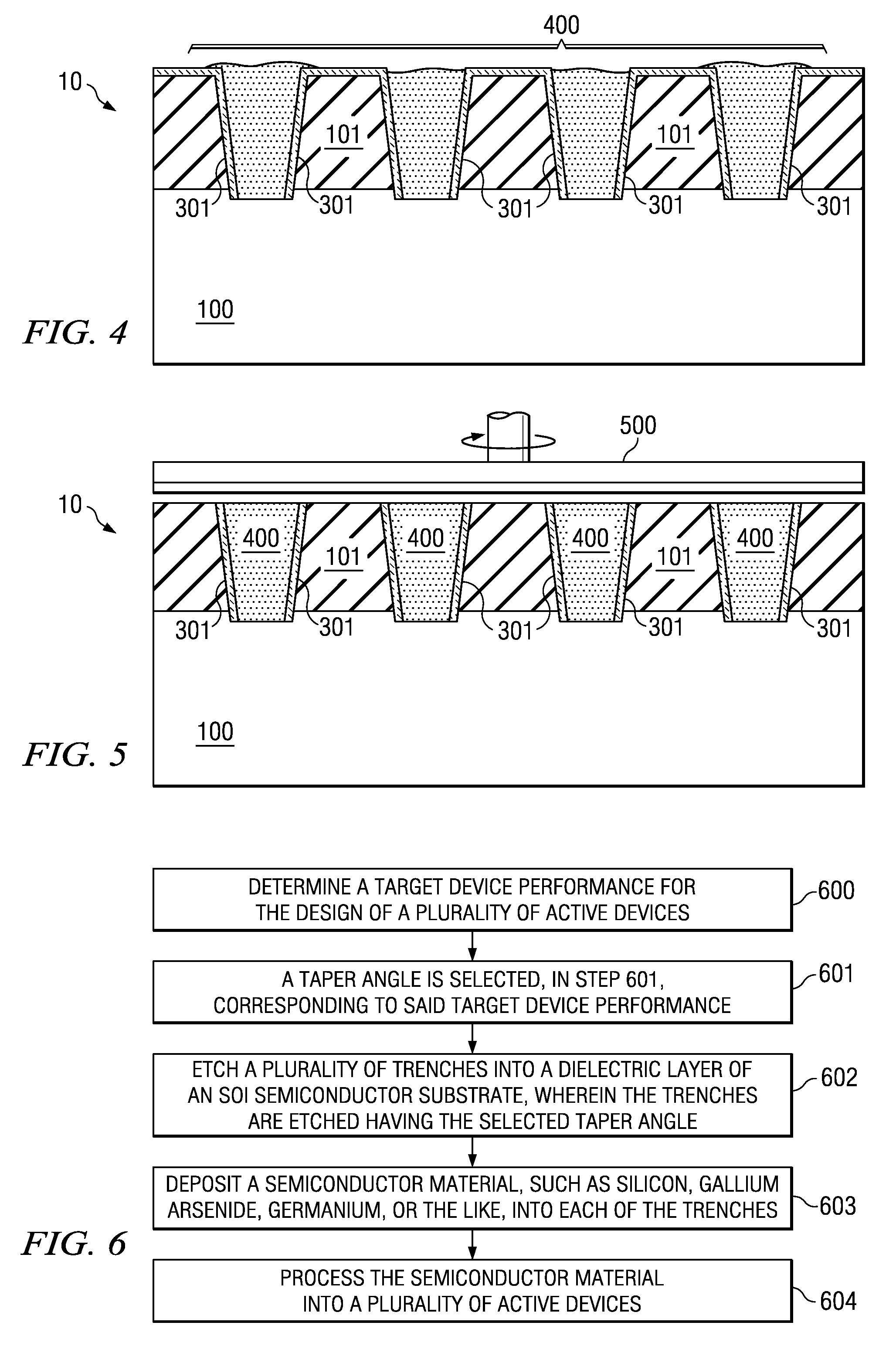
[0014]Turning now to FIG. 1, semiconductor wafer 10 is shown in a first processing step configured according to one embodiment of the present invention. Semiconductor wafer 10 comprises substrate 100. Substrate 100 may be made from a semiconductor substrate material such as silicon, gallium arsenic, germanium, or the like. In a first processing step, dielectric layer 101 is deposited on top of substrate 100. Dielectric layer 101 may be made from various dielectric materials, such as silicon dioxide, silicon nitride, and the like, and may have any suitable dielectric constant,...
PUM
 Abstract
Description
Claims
Application Information