Method of patterning color conversion layer and method of manufacturing organic el display using the patterning method

a technology of color conversion layer and organic el, which is applied in the manufacture of electrode systems, electric discharge tubes/lamps, discharge tubes luminescnet screens, etc., can solve the problems of reducing yield, affecting the quality of organic el, etc., to achieve high-definition display, easy and economical manufacturing, and large surface area

Active Publication Date: 2009-09-17
SHARP KK
View PDF18 Cites 18 Cited by
  • Summary
  • Abstract
  • Description
  • Claims
  • Application Information

AI Technical Summary

Benefits of technology

[0016]The forming the color conversion layer and the patterning the color conversion layer are preferably carried out in an inline vacuum process in order to maximize quality and yield. The inline vacuum process moves work pieces between various process stations while maintaining a vacuum. The inline vacuum process provides superior results over loading work pieces into separate containers (usually containing an inert gas), moving the containers to the next process station, and then unloading the work pieces at the next process station.
[0028]By using the patterning method according to the invention the color conversion layer can be formed as a continuous film (a solid film) when depositing the color conversion layer. Therefore, there is no necessity for the use of a metal mask which causes problems in precision and resolution as found in conventional processes. Thus, the color conversion layer can be formed into a fine pattern having a pixel resolution that could not be obtained by previous methods. In addition, the invention can produce displays having a large surface area also previously unobtainable by conventional methods. For example, while a conventional metal mask may be able to produce arrays up to 550 mm×650 mm, the invention can produce arrays of much larger dimensions including arrays having at least one dimension greater than 650 mm. As a result, a high definition display can be easily and economically manufactured by patterning the color conversion layer in accordance with the invention.

Problems solved by technology

It has been reported that in such a device the balance in light emitting intensity among light emitting materials varies, which causes possible changes in hues that are obtained.
However, although the method of forming a deposition pattern using a metal mask has long been known, in preparing finer mask patterns, limitation in the material and the thickness of the mask limits the level of definition of the mask pattern to 150 to 200 pixels per inch (ppi).
Attempting to provide pattern with a definition higher than 150 to 200 ppi, results in problems of increasing complexity, makes it impossible to obtain a higher definition pattern for a large area, and also results in a reduction in yield.
For example, the thickness required for a metal mask is around 50 microns in order to provide sufficient strength, but this thickness limits the size of potential openings in the metal mask pattern.
Further, differences in the thermal expansion coefficients between the metal mask and the substrate cause alignment problems.
Large size metal masks (for example on the order of 730 mm×920 mm) may be misaligned up to several tens of microns due to flexing and expansion problems.
However, for a color conversion layer formed by deposition or formed only of dyes, it would be difficult to form a desired pattern because of lack of fluidity and a small thickness, on the submicron order, of the color conversion layer.

Method used


Image

  • Method of patterning color conversion layer and method of manufacturing organic el display using the patterning method
  • Method of patterning color conversion layer and method of manufacturing organic el display using the patterning method
  • Method of patterning color conversion layer and method of manufacturing organic el display using the patterning method

Examples


example 1

[0077]According to procedures in the following processes (1) to (8), a multiple color light emitting organic EL display according to the invention was produced.

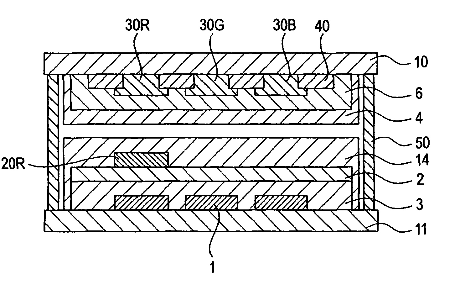
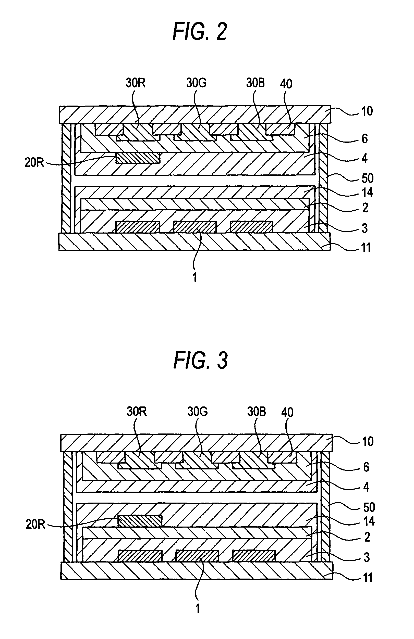
(1) Formation of the Color Filter Layer 30

[0078]With 1737 glass (manufactured by Corning Inc.) used as the transparent substrate 10, and with black matrix material (CK-7001: manufactured by FUJIFILM Electronic materials Co., Ltd.), red color filter layer material (CR-7001: manufactured by FUJIFILM Electronic materials Co., Ltd.), green color filter layer material (CG-7001: manufactured by FUJIFILM Electronic materials Co., Ltd.) and blue color filter layer material (CB-7001: manufactured by FUJIFILM Electronic materials Co., Ltd.) used thereon, the black matrix 40 and the color filter layers 30R, 30G and 30B are formed thereon. The thickness of each layer was 1 μm.

[0079]The dimensions of each of the sub-pixels of the formed color filter layer were 100 μm×30 μm and the spacing between the sub-pixels (namely the inter-pixel spa...

examples 2 , 3 and 4

Examples 2, 3 and 4, and Comparison Example 5

[0091]In the patterning of the color conversion layer 20, with the processes made similar to those in the example 1 except that the respective heating temperatures of the mold 84 were changed, organic EL displays of examples 2, 3 and 4 and comparison example 5 were obtained.


PUM

PropertyMeasurementUnit
widthaaaaaaaaaa
thicknessaaaaaaaaaa
thicknessaaaaaaaaaa

Abstract

A method of patterning a color conversion layer for an organic EL device is provided together with a method of manufacturing a multiple color emitting organic EL display using the patterning method. The patterning method includes forming the color conversion layer on a base having an organic layer and patterning the color conversion layer by carrying out a thermal cycle nano imprint technique.

Description

CROSS REFERENCE TO RELATED APPLICATIONS[0001]This application claims priority from Japanese Patent Application No. JP 2007-013579, filed on Jan. 24, 2007, the contents of which are incorporated herein by reference in their entirety.TECHNICAL FIELD[0002]The present invention relates to a method of patterning a color conversion layer in an organic EL display. The invention also relates to a method of manufacturing an organic EL display that emits light of at least one of the primary colors, in which a color conversion layer is patterned with a pixel shape using the aforementioned method of patterning a color conversion layer.BACKGROUND ART[0003]Active studies have been carried out in recent year regarding the commercialization of organic EL devices. An organic EL device enables a high current density with a low applied voltage to achieve the realization of high light emitting luminance and high light emission efficiency. Therefore, commercialization of a multiple-color light emission ...

Claims


Application Information

Patent Timeline
Patent Type & Authority Applications(United States)
IPC IPC(8): H01J1/62H05H1/26B28B11/08H01J9/227
CPCH01L51/0014H01L27/322H10K59/38H10K71/20
Inventor KANAI, NAOYUKI
Owner SHARP KK
Why Eureka
Try Eureka