Variable resistor element and its manufacturing method

a technology of resistor elements and manufacturing methods, applied in the direction of varistor cores, thin film varistors, instruments, etc., can solve problems such as far from ideal

Inactive Publication Date: 2009-09-17
SHARP KK +1
View PDF3 Cites 25 Cited by
  • Summary
  • Abstract
  • Description
  • Claims
  • Application Information

AI Technical Summary

Benefits of technology

[0033]According to the variable resistor element having the above characteristics or the manufacturing method of the variable resistor element having the above characteristics, since the switching operation principle by the metal-insulator transition (Mott transition) at the interface between a first electrode that is either one of the two metal electrodes and the variable resistor is theoretically shown, a material design condition to provide the appropriate switching operation becomes clear, so that the variable res

Problems solved by technology

However, each above memory device has good and bad points and it is far from an

Method used


Image

  • Variable resistor element and its manufacturing method
  • Variable resistor element and its manufacturing method
  • Variable resistor element and its manufacturing method

Examples


first embodiment

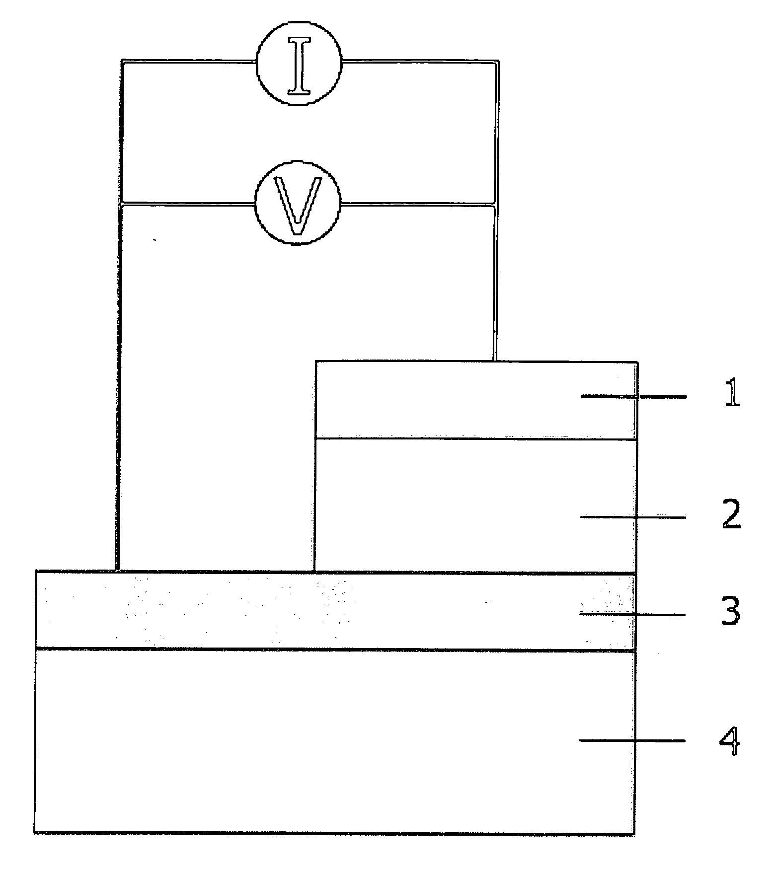
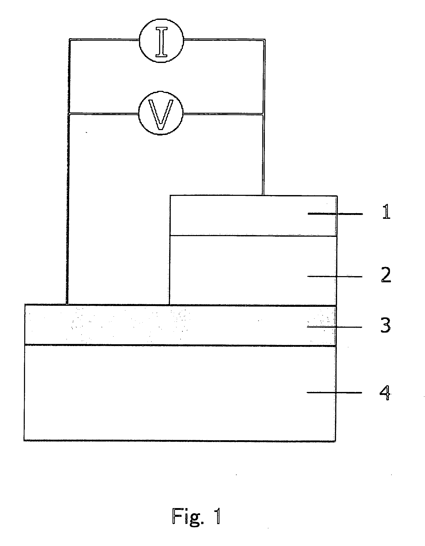
[0062]FIG. 1 is a sectional view showing a sectional structure of an element of the present invention according to a first embodiment. The element of the present invention is formed by sequentially depositing a lower electrode 3, a variable resistor 2 formed of a strongly-correlated material (strongly-correlated electron material) of a p-type semiconductor, and an upper electrode 1 on a substrate 4. The variable resistor 2 in a metal state is sandwiched between the electrodes 1 and 3 and it is operated by applying a voltage pulse between the electrodes. The switching operation between an ON state (low resistance state) and OFF state (high resistance state) is implemented by the voltage pulse having a voltage magnitude greater than that of an absolute value of a threshold voltage as will be described below, and the resistance state of the element of the present invention is read by applying a voltage lower than the threshold voltage to use the element as a memory element. To provide ...

second embodiment

[0083]FIG. 8 shows a sectional structure of an element of the present invention according to a second embodiment. The element of the present invention is provided by sequentially depositing a lower electrode 3, a variable resistor 5 formed of a strongly-correlated material of an n-type semiconductor, and an upper electrode 1 on a substrate 4. The variable resistor 2 in a metal state is sandwiched between both electrodes 1 and 3 and it is operated by applying a voltage pulse between the electrodes. The switching operation between an ON state (low resistance state) and OFF state (high resistance state) is implemented by the voltage pulse having a voltage magnitude greater than that of an absolute value of a threshold voltage as will be described below, and the resistance state of the element of the present invention is read by applying a voltage lower than the threshold voltage to use the element as a memory element. To provide different electric resistances between the ON state and O...

third embodiment

[0096]According to the present invention, a strongly-correlated material of the variable resistor other than the perovskite-type oxide described in the above first and second embodiments can cause the similar resistance switching operation by introducing an oxygen defect or introducing excessive oxygen. One example thereof includes a binary oxide such as NiO and CoO in which the oxygen defect or excessive oxygen is introduced. Since the material has small number of metal elements, adjustment of composition is easy. In addition, Fe3O4 and the like are preferable. Furthermore, a material such as VO2, V2O3 or Cr-doped V2O3 is also preferable. Similarly, a material such as TiO2 or TinO2n−1 (n=2, 3) is preferable.

[0097]In addition, when the excessive oxygen is introduced, a hole is introduced as a carrier to be the p-type semiconductor. Thus, when a potential difference Vd defined by a difference between the work function of the electrode material and the work function of the variable re...


PUM


Abstract

A variable resistance element comprises a variable resistor of strongly-correlated material sandwiched between two metal electrodes, and the electric resistance between the metal electrodes varies when a voltage pulse is applied between the metal electrodes. Such a switching operation as the ratio of electric resistance between low and high resistance states is high can be attained by designing the metal electrodes and variable resistor appropriately based on a definite switching operation principle. Material and composition of the first electrode and variable resistor are set such that metal insulator transition takes place on the interface of the first electrode in any one of two metal electrodes and the variable resistor by applying a voltage pulse. Two-phase coexisting phase of metal and insulator phases can be formed in the vicinity of the interface between the variable resistor and first electrode by the work function difference between the first electrode and variable resistor.

Description

CROSS-REFERENCE TO RELATED APPLICATIONS[0001]This application is a National Phase filing under 35 U.S.C. § 371 of International Application No. PCT / JP2006 / 315649 filed on Aug. 8, 2006, and which claims priority to Japanese Patent Application No. 2005-247071 filed on Aug. 29, 2005.TECHNICAL FIELD[0002]The present invention relates to a variable resistor element provided with a variable resistor sandwiched between two metal electrodes and changing an electric resistance between the metal electrodes when a voltage pulse is applied between the metal electrodes, and its manufacturing method.BACKGROUND ART[0003]Recently, as a next-generation NVRAM (Nonvolatile Random Access Memory) capable of operating at high speed to replace a flash memory, various kinds of device structures such as a FeRAM (Ferroelectric RAM), a MRAM (Magnetic RAM), an OUM (Ovonic Unified Memory) are proposed and a fierce development race is carried on in terms of implement high performance, high reliability, low cost,...

Claims


Application Information

Patent Timeline
IPC IPC(8): H01C7/10
CPCG11C13/0007G11C2213/15G11C2213/31H01C7/1013H01L45/147H01L45/04H01L45/1233H01L45/146H01C7/115H10N70/20H10N70/826H10N70/8833H10N70/8836
Inventor HOSOI, YASUNARIOHNISHI, SHIGEOOGIMOTO, YASUSHIOKA, TAKASHINAGAOSA, NAOTOTOKURA, YOSHINORI
Owner SHARP KK
Why Eureka
Try Eureka