Variable resistor element, manufacturing method thereof, and memory device provided with it

a technology of resistor elements and manufacturing methods, which is applied in the direction of solid-state devices, semiconductor devices, instruments, etc., can solve the problems of large programming current (several ma) according to non-patent document 3 using nio, small resistance change, and incompatibility with conventional cmos processes. achieve stable switching operation, high compatibility, and data retaining characteristics are preferable

Inactive Publication Date: 2010-04-08
SHARP KK
View PDF5 Cites 15 Cited by
  • Summary
  • Abstract
  • Description
  • Claims
  • Application Information

AI Technical Summary

Benefits of technology

[0023]According to the variable resistor element comprising the variable resistor formed of the oxynitride of the transition metal element in the present invention, a stable switching operation is provided and data retaining characteristics are preferable.
[0024]When the variable resistor element according to the present invention is used, since noble metal is not always needed as the electrode material, the variable resistor element has high compatibility with an existing CMOS process and easily manufactured.
[0025]In addition, according to the variable resistor element in the present invention, the variable resistor material can be formed by oxidizing the lower electrode surface comprising the conductive nitride. According to the manufacturing method, since the variable resistor film can be formed in a heat treatment process for oxidation that is a general process in a semiconductor process, a special device to form the film is not needed.
[0026]Furthermore, according to the memory device comprising the variable resistor element in the present invention, since the memory device having preferable data retaining characteristics can be implemented by the stable switching operation having a large resistance ratio, it can be applied to a recording medium of an electronic device such as a memory card, a mobile telephone, a mobile game, a digital camera, and a printer.

Problems solved by technology

However, when a perovskite-type oxide is used as the material of the variable resistor 2 changing its resistance by the voltage pulse, the resistance change is small and the stable switching operation is not provided depending on the material, or it is necessary to use a noble metal electrode having good lattice compatibility with the perovskite-type oxide and high conductivity and high resistance to oxidation as the lower electrode 3, which is bad in compatibility with a conventional CMOS process.
In addition, when the oxide of the transition metal element is used as the material of the variable resistor 2, the problem is that a programming current is large (several mA) according to the non-patent document 3 using NiO, for example.

Method used


Image

  • Variable resistor element, manufacturing method thereof, and memory device provided with it
  • Variable resistor element, manufacturing method thereof, and memory device provided with it
  • Variable resistor element, manufacturing method thereof, and memory device provided with it

Examples


example 1

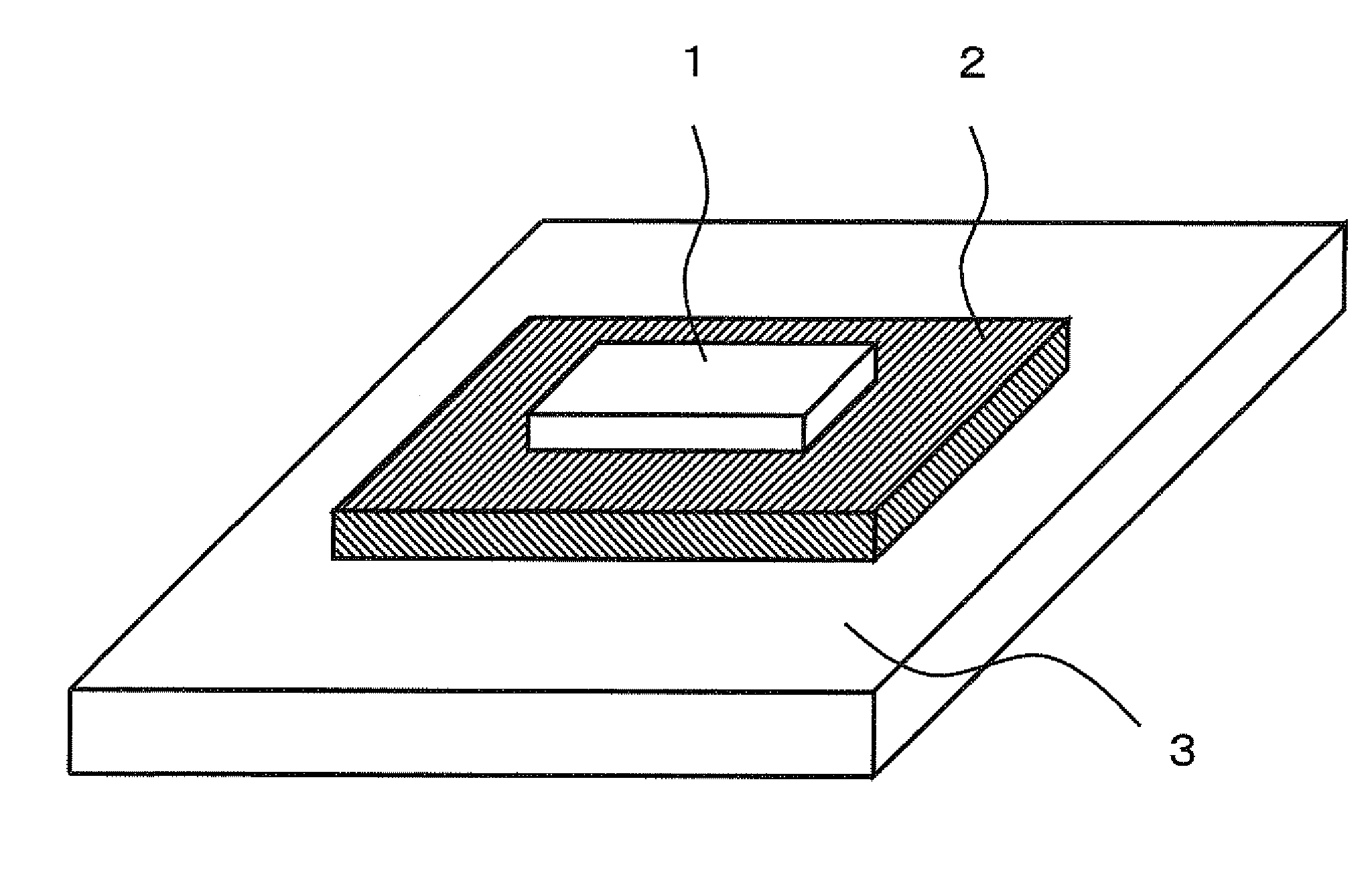
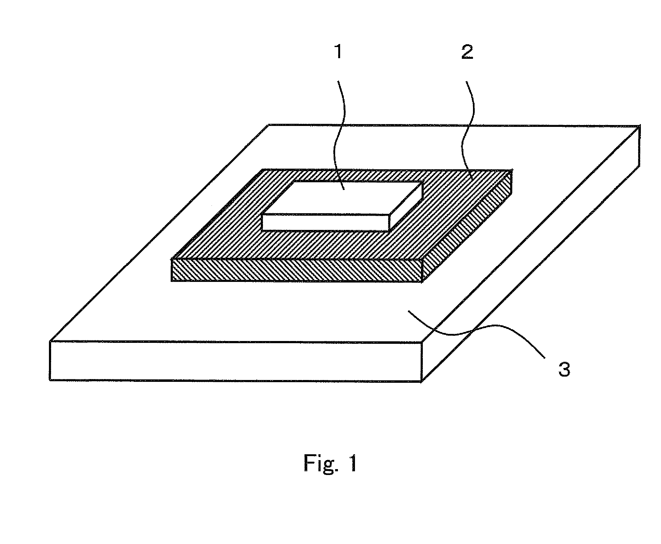
[0084]According to a variable resistor element in a first embodiment of the present invention, a variable resistor 2 comprising an oxynitride of a transition metal element is formed of a TiON (titanium oxynitride) film. A specific example of the first embodiment will be described as an example 1 hereinafter.

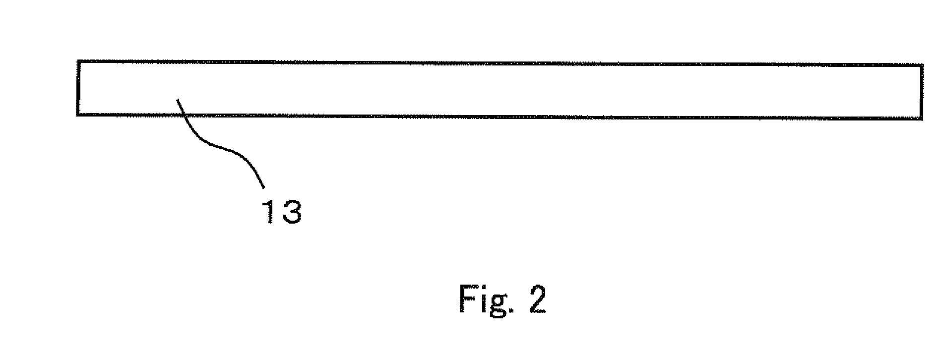
[0085]FIG. 7 is a schematic sectional view showing a variable resistor element regarding the example 1 of the present invention. This variable resistor element comprises a second electrode 13 serving as a lower electrode, a variable resistor 12, and a first electrode 11 serving as an upper electrode laminated sequentially in a direction perpendicular to a substrate. In addition, in order to apply a voltage pulse to the first electrode 11 and the second electrode 13, a contact hole 15 is formed in an interlayer insulation film 14 and a metal wiring 16 is provided. The variable resistor element can be manufactured through the following processes.

[0086]First, as shown in FIG. 2, the...

example 2

[0111]A variable resistor element according to a second embodiment of the present invention has the same constitution as that of the variable resistor element of the first embodiment shown FIGS. 2 to 7. However, a manufacturing method of a variable resistor 12 is different from that of the variable resistor element in the first embodiment. That is, while the variable resistor material film 12 comprising the oxynitride of the transition metal element is formed by performing the oxidation treatment on the surface of the conductive nitride 13 of the lower electrode in the first embodiment, the variable resistor material film 12 is formed by CVD method in the second embodiment of the present invention. This will be described as an example 2 in detail hereinafter.

[0112]The variable resistor element in the example 2 can be manufactured by the following processes.

[0113]First, as shown in FIG. 2 similar to the example 1, a Pt film 13 having a film thickness of 200 nm is deposited on a base ...

example 3

[0119]According to a third embodiment of the present invention, a description will be made of a memory device comprising the variable resistor element formed of the oxynitride of the transition metal element described above in detail. The third embodiment will be described as an example 3.

[0120]FIG. 14 is a schematic block diagram showing one embodiment of a memory device 30 according to the present invention. The memory device 30 of the present invention comprises a control circuit 32, a reading circuit 33, a bit line decoder 34, a word line decoder 35, and a voltage pulse generation circuit 36 as peripheral circuits of a memory cell array 31.

[0121]The control circuit 32 controls programming, erasing and reading of the memory cell array 31. Data is stored in a specific memory cell corresponding to an address signal in the memory cell array 31, and the data is outputted to an external device through the reading circuit 33. The control circuit 32 controls the bit line decoder 34, the...


PUM

PropertyMeasurementUnit
areaaaaaaaaaaa
thicknessaaaaaaaaaa
thicknessaaaaaaaaaa

Abstract

A variable resistor element comprising a first electrode, a second electrode, and a variable resistor positioned between the first and second electrodes, and changing in electric resistance when a voltage pulse is applied between the both electrodes, has posed problems that it has a restriction of having to use noble metal electrodes as an electrode material and is not compatible with a conventional CMOS process. A variable resistor element using an oxynitride of transition metal element as a variable resistor exhibits a stable switching operation, is satisfactory in data retaining characteristics, and requires a small programming current. Since it does not necessarily require noble metal as an electrode material, it is high in compatibility with the existing CMOS process and easy to produce. It can be formed by a simple step of forming a variable resistor material into a film by oxidizing a lower electrode surface consisting of conductive nitride.

Description

CROSS-REFERENCE TO RELATED APPLICATIONS[0001]This application is a National Phase filing under 35 U.S.C. § 371 of International Application No. PCT / JP2006 / 314487 filed on Jul. 21, 2006, and which claims priority to Japanese Patent Application No. 2005-228600 filed on Aug. 5, 2005.TECHNICAL FIELD[0002]The present invention relates to a variable resistor element comprising a first electrode, a second electrode, and a variable resistor sandwiched between the first electrode and the second electrode and having an electric resistance changed when a voltage pulse is applied between both electrodes, and its manufacturing method. In addition, the present invention relates to a memory device comprising the variable resistor element.BACKGROUND ART[0003]Recently, as a next-generation NVRAM (Nonvolatile Random Access Memory) capable of operating at high speed to replace a flash memory, various kinds of device structures such as a FeRAM (Ferroelectric RAM), a MRAM (Magnetic RAM), an OUM (Ovonic ...

Claims


Application Information

Patent Timeline
Patent Type & Authority Applications(United States)
IPC IPC(8): H01L27/10H01C17/00
CPCG11C13/0007G11C13/0026G11C2213/52G11C2213/79H01L45/145Y10T29/49082H01L45/1233H01L45/1633H01L45/1675H01L27/2436H01L45/04H10B63/30H10N70/20H10N70/826H10N70/883H10N70/028H10N70/063H01L27/10H10N70/00H10N99/00
Inventor HOSOI, YASUNARI
Owner SHARP KK
Why Eureka
Try Eureka