Manufacturing method for variable resistive element

a technology of resistive elements and manufacturing methods, which is applied in the manufacturing of basic electric elements, semiconductor/solid-state devices, electrical equipment, etc., can solve the problems of inability to say that the surface is always clean and the contact resistance is not stable, and achieve the effect of stabilizing contact resistance and stable switching properties

Active Publication Date: 2009-11-10
XENOGENIC DEV LLC
View PDF6 Cites 9 Cited by
  • Summary
  • Abstract
  • Description
  • Claims
  • Application Information

AI Technical Summary

Benefits of technology

[0018]The present invention is provided in view of the above described problems, and an object thereof is to provide a manufacturing method for a variable resistive element having a stable switching operation with excellent reproducibility.

Problems solved by technology

In accordance with conventional methods, however, the surface of the electrodes and the variable resistor is exposed to gases and chemicals used in the process, therefore, it cannot be said that the surface is always clean.
In addition, a problem arises, such that the contact resistance is not stable, due to the effects of natural oxidation after the film formation of the lower electrodes and variable resistors, and the effects of the atmosphere on the process for film formation for the films deposited in upper layers.

Method used


Image

  • Manufacturing method for variable resistive element
  • Manufacturing method for variable resistive element
  • Manufacturing method for variable resistive element

Examples


first embodiment

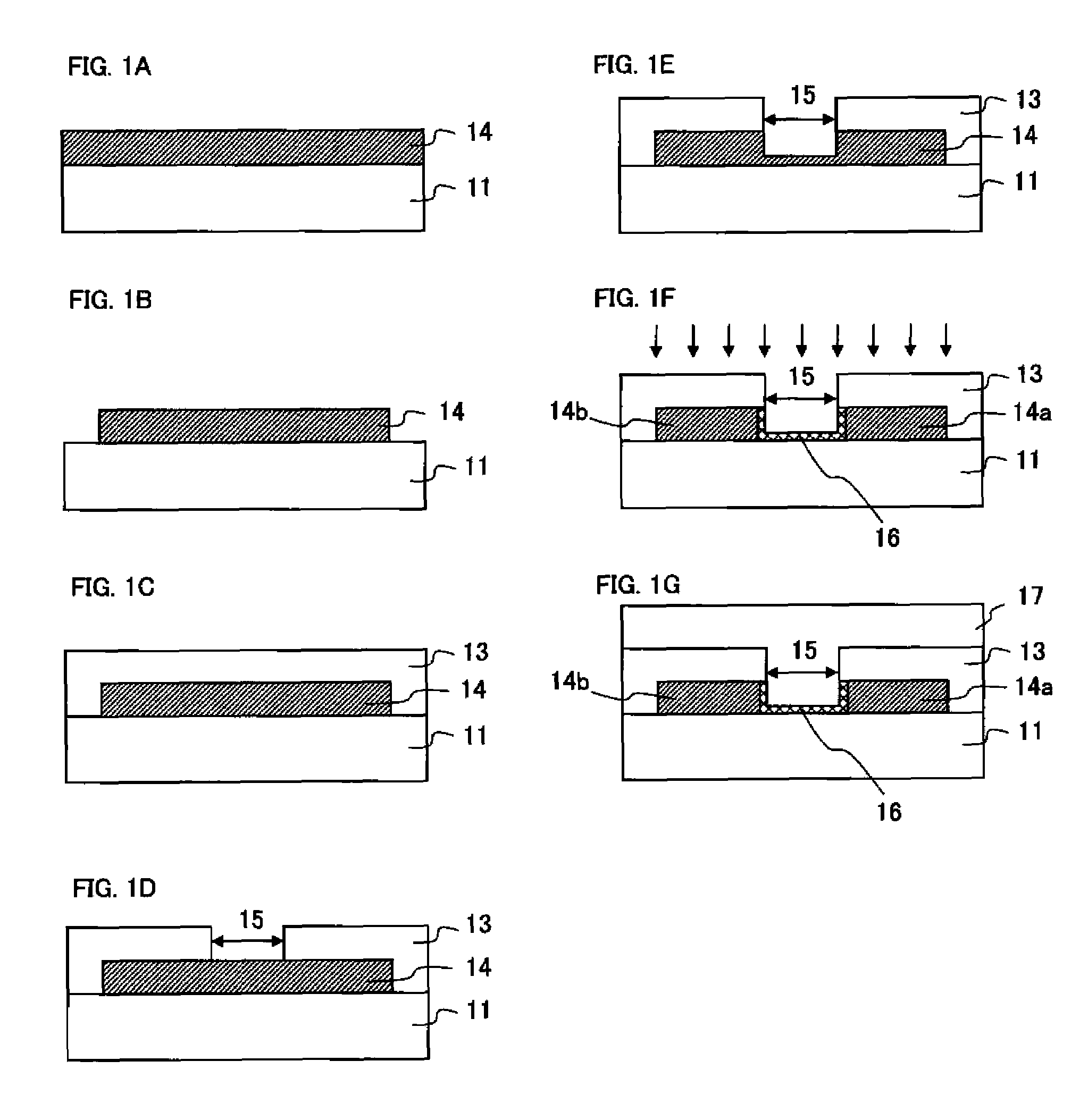
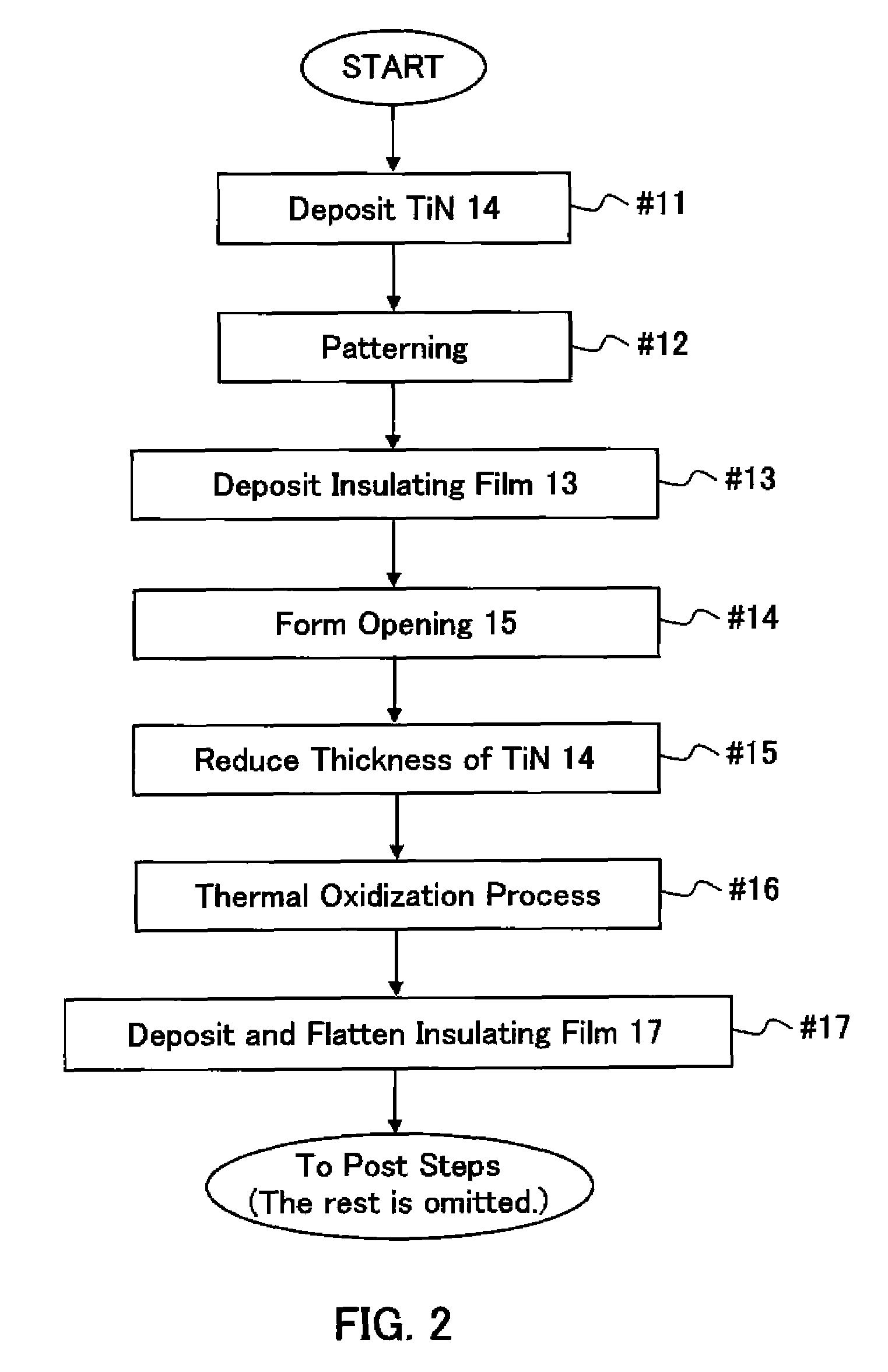
[0090]The first embodiment of the method of the present invention (hereinafter referred to as “present embodiment”) is described in reference to FIGS. 1A to 1G and FIG. 2. FIGS. 1A to 1G are cross sectional diagrams schematically illustrating the steps for the manufacture of a semiconductor device according to the present embodiment, respectively. In addition, FIG. 2 is a flow chart illustrating the manufacturing steps in the present embodiment, and each step in the following corresponds to a step in the flow chart of FIG. 2.

[0091]Here, the schematic cross sectional diagrams of FIGS. 1A to 1G and other schematic structural diagrams which are referred to for the description of the present and following respective embodiments are shown solely for the purpose of illustration, and thus, the scale of the dimensions of the actual structure and that of the drawings do not necessarily coincide. In addition, the numerical values of the film thickness of the respective films deposited in the ...

second embodiment

[0106]The method according to the second embodiment (hereinafter referred to as “present embodiment”) of the present invention is described below in reference to FIGS. 3A to 3G and 4. FIGS. 3A to 3G are cross sectional diagrams schematically illustrating the steps for the manufacture of a semiconductor device according to the present embodiment, respectively. In addition, FIG. 4 is a flow chart showing the manufacturing steps according to the present embodiment, and the respective steps in the following represent the respective steps in the flow chart shown in FIG. 4.

[0107]First, as shown in FIG. 3A, an SiO2 film (first interlayer insulating film) 13 is deposited on the entire surface of the semiconductor substrate 11 where an appropriate transistor circuit or the like (not shown) is formed in accordance with a CVD method so as to have a thickness of 100 nm (Step #21).

[0108]Next, as shown in FIG. 3B, the first interlayer insulating film 13 is patterned in accordance with a well-know...

third embodiment

[0115]The method according to the third embodiment (hereinafter referred to as “present embodiment”) of the present invention is described below in reference to FIGS. 5A to 8. FIGS. 5A to 5E are cross sectional diagrams schematically illustrating the steps for the manufacture of a semiconductor device according to the present embodiment, respectively. In addition, FIG. 6 is a flow chart showing the manufacturing steps according to the present embodiment, and the respective steps in the following represent the respective steps in the flow chart shown in FIG. 6.

[0116]First, as shown in FIG. 5A, an SiO2 film (first interlayer insulating film) 13 is deposited over the entire surface of the semiconductor substrate 11 where an appropriate transistor circuit or the like (not shown) and a metal wiring 21 are formed in accordance with a CVD method so as to have a thickness of 400 nm (Step #31).

[0117]Next, as shown in FIG. 5B, the first interlayer insulating film 13 is patterned in accordance...


PUM


Abstract

A manufacturing method for a variable resistive element according to which a stable switching operation can be achieved with excellent reproducibility is provided. A conductive thin film is deposited on a semiconductor substrate and patterned to a predetermined form, and after that, a first interlayer insulating film is deposited. An opening is then created in a predetermined location on the first interlayer insulating film in such a manner that the upper surface of the conductive thin film is exposed and the thickness of the conductive thin film formed at the bottom of this opening is reduced through processing, and after that, an oxidation process is carried out on the periphery of the exposed conductive thin film. As a result, a variable resistor film is formed in the peripheral region of the opening, and this variable resistor film divides the conductive thin film into a first electrode and a second electrode.

Description

BACKGROUND OF THE INVENTION[0001]1. Field of the Invention[0002]The present invention relates to a manufacturing method for a variable resistive element having two electrodes and a variable resistor where the above described variable resistor is in such a region as to be sandwiched between the two electrodes, and the electrical resistance changes when a voltage pulse is applied between the two electrodes.[0003]2. Description of the Related Art[0004]In recent years, various device structures, such as FeRAM's (ferroelectric RAM's), MRAM's (magnetic RAM's) and PRAM's (phase change RAM's) have been proposed as next generation nonvolatile random access memories (NVRAM's), which make fast operation possible and substitute for flash memories, and severe competition in development has led to improvement in the performance, increase in the reliability, reduction in cost and improvement in the integration in the manufacturing process. These memory devices presently have both advantages and sh...

Claims


Application Information

Patent Timeline
Patent Type & Authority Patents(United States)
IPC IPC(8): H01L21/20
CPCH01L45/1226H01L45/124H01L45/146H01L45/04H01L45/1633H10N70/823H10N70/8265H10N70/20H10N70/8833H10N70/028
Inventor INOUE, YUSHIOHNISHI, TETSUYAISHIHARA, KAZUYASHIBIUYA, TAKAHIROHOSOI, YASUNARIYAMAZAKI, SHINOBUNAKANO, TAKASHI
Owner XENOGENIC DEV LLC
Why Eureka
Try Eureka