
Micromachine and manufacturing method therefor

Inactive Publication Date: 2004-06-29
SEIKO EPSON CORP
View PDF13 Cites 4 Cited by
  • Summary
  • Abstract
  • Description
  • Claims
  • Application Information

AI Technical Summary

Benefits of technology

Further, another object of the present invention is to provide a configuration, by which a micromachine having a drive system can be manufactured, and to provide a manufacturing method therefor.
Further, the second microstructured portion, from which light is extracted, is formed from the resin. Thus, as compared with the case of employing glass material, the hardness is low. Moreover, the flatness of the light extraction surface can be ensured by the mold transfer. This results in an increase in the adherence between the surface (namely, extraction surface) of the second microstructured portion and the surface of the light guiding portion adapted to guide light by performing the total reflection of the light. Thus, the micromachine of the present invention can provide a more stable switching operation and a high contrast spatial light modulator.

Problems solved by technology

However, this optical switching element using liquid crystals is poor in high-speed response, and operates at a response speed of as low as about several millimeters per second.
It is, therefore, difficult to use a spatial light modulator, which employs liquid crystals, in optical communication, optical computing, an optical storage device such as a hologram memory, and an optical printer, which require a high response speed.
Further, the spatial light modulator employing liquid crystals has a drawback in that efficiency in using light is degraded by the polarizing plates.
Thus, although a structure constituted by a micromachine is produced by these manufacturing methods, the necessary surface accuracy of a microstructure, which is less than the tolerance thereof, cannot be necessarily ensured.
Moreover, it is difficult to assure the positional relationship among a plurality of switching elements with precision of one-tenth of several microns or less.
Thus, even in the case of using the photolithography techniques, it is difficult to process other materials, for example, a transmissive resin material suitable for an optical element.
Similar problems occur in other micromachines, such as an optical micro-switch for switching on and off signals transmitted between optical fibers, and a microvalve for allowing fluids to flow therethrough and shutting off the fluids.
However, in the case of using the mold transfer method, the surface accuracy of the microstructure can be ensured, while the drive system itself including a spring or a film cannot be manufactured in the micromachine.
Moreover, as long as the mold transfer is employed, there is a little limit to the material.
On the other hand, there is the possibility that the first microstructured portion produced in the micromachine by performing this process is broken by stress generated when the second microstructure is formed on the first microstructure by the mold transfer.

Method used


Image

  • Micromachine and manufacturing method therefor
  • Micromachine and manufacturing method therefor
  • Micromachine and manufacturing method therefor

Examples


Embodiment Construction

Spatial Light Modulator

Hereinafter, the present invention will be described in more detail by describing an example of the manufacture of a spatial light modulator.

Outline of Configuration of Spatial Light Modulator

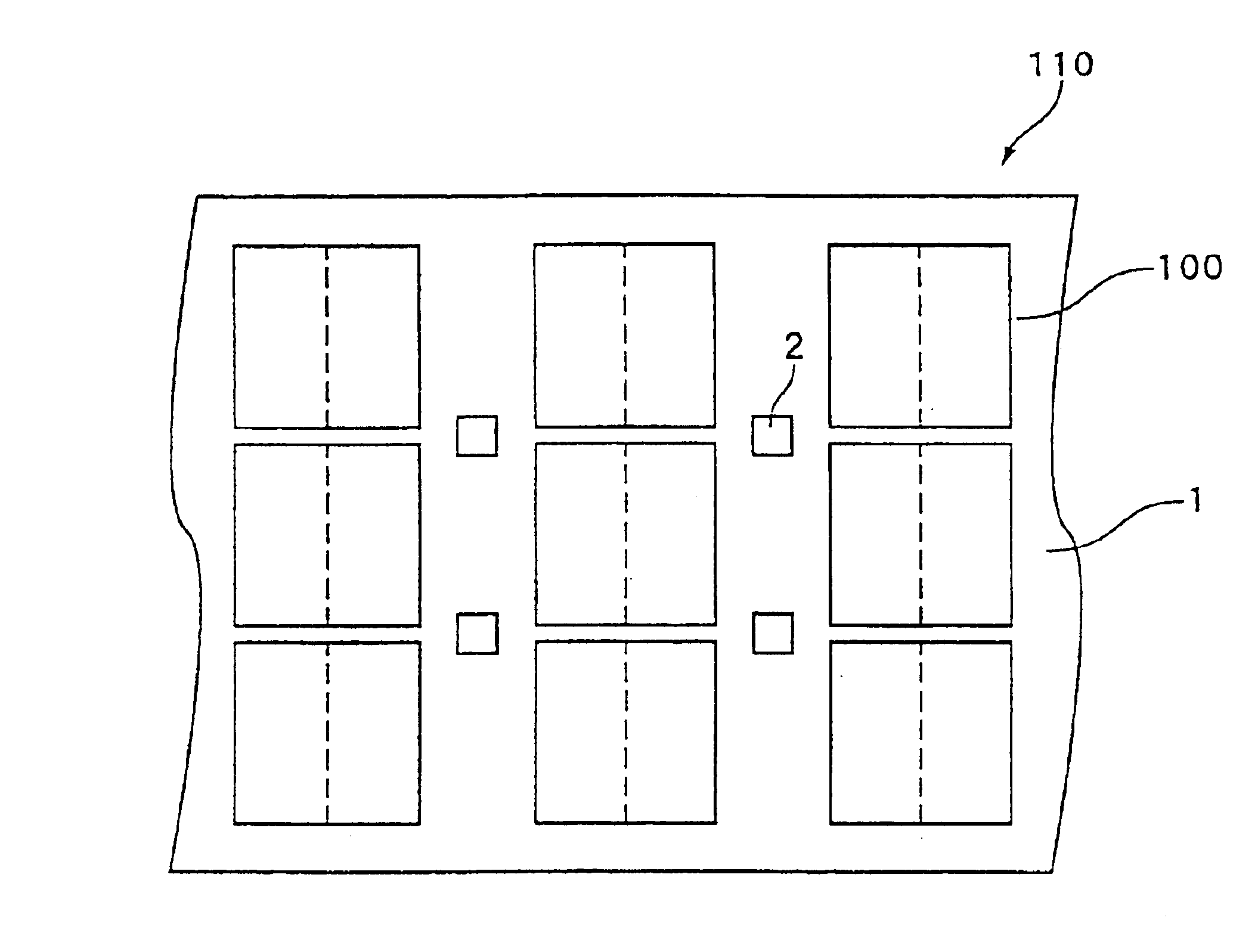
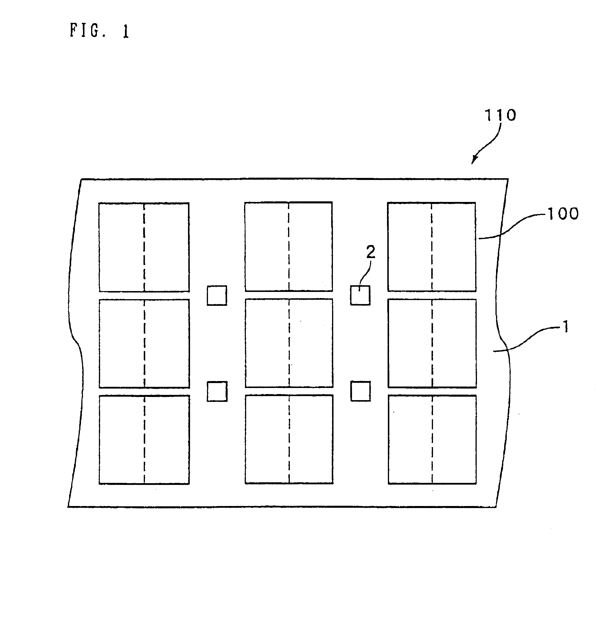
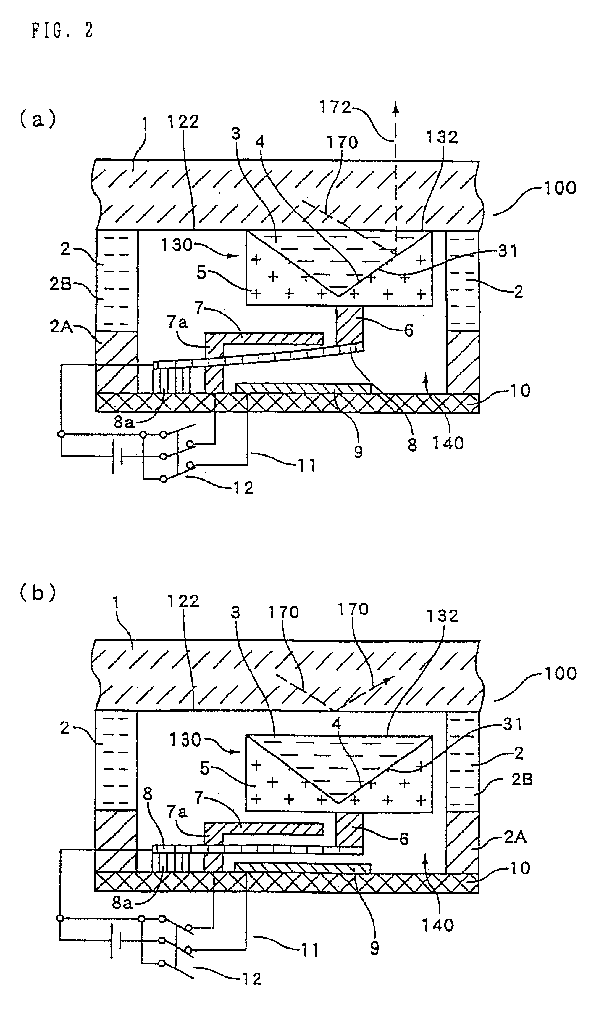
In a spatial light demodulator 110 of this example, a plurality of switching elements 100 are arranged in a two-dimensional array, as illustrated in FIG. 1. In the case that an image is represented by this spatial light modulator 110, each of the switching elements at 100 is a switching device adapted to function as a pixel. FIGS. 2(a)-(b) illustrates an outline of the configuration of the switching element 100 by picking out one of the switching elements 100 and using a sectional representation thereof. The optical switching element 100 of this example is operative to extract evanescent light by bringing a switching portion 130, which has a transmissive extraction surface, into contact with the total reflection surface (namely, the bottom surface) of the light guiding po...


PUM

PropertyMeasurementUnit
Pressureaaaaaaaaaa
Shapeaaaaaaaaaa
Microstructureaaaaaaaaaa

Abstract

A micromachine and a manufacturing method are provided for a micromachine that has a dynamic first microstructured portion serving as a drive portion, and a static second microstructured portion adapted to perform a switching function and which functions as an optical element. The second microstructured portion can be manufactured at least without complex steps, such as a silicon process, by forming a static second microstructure on the dynamic first microstructured portion, or in such a way as to be overlaid thereon by mold transfer. Thus, the microstructured portion of a complex shape can be easily formed with good reproducibility. When a plurality of elements are arranged in an array, similarly as in the case of a spatial light modulator, the stable reproduction thereof is achieved by the mold transfer. Thus, as compared with the case of manufacturing all elements in a silicon process, the probability of an occurrence of a defect is very low.

Description

1. Field of the InventionThe present invention relates to a micromachine, such as an optical switching element for use in an image display device, and to a manufacturing method therefor.2. Description of Related ArtAn optical switching element using liquid crystals has been known as that enabled to control the switching-on and switching-off of light. FIG. 13 schematically shows the configuration thereof. This optical switching element 900 may consist of polarizing plates 901 and 908, glass plates 902 and 903, transparent electrodes 904 and 905, and liquid crystals 906 and 907. The direction of alignment of liquid crystal molecules is changed by controlling a voltage applied between the transparent electrodes 904 and 905. Thus, the plane of polarization thereof is turned thereby to perform optical switching. Consequently, an image display device can be constituted as a liquid crystal panel by arranging such optical switching elements (namely, liquid crystal cells) in a two-dimensiona...

Claims


Application Information

Patent Timeline
IPC IPC(8): B81B3/00G02B26/02B81C1/00
CPCB81C1/00182G02B26/02B81B2201/045B81C2201/034B81B3/00B81C1/00
Inventor KAMIJIMA, SHUNJIYONEKUBO, MASATOSHITAKEDA, TAKASHINISHIKAWA, TAKAO
Owner SEIKO EPSON CORP
Learn More