
Device for ESD protection of an integrated circuit

a technology of integrated circuits and devices, applied in the direction of overvoltage protection resistors, emergency protective arrangements for limiting excess voltage/current, and arrangements responsive to excess voltage, etc., can solve problems such as noise, integrated electrostatic discharges may damage electronic devices, and series resistance at normal operating voltages may be too high, so as to achieve a larger resistance ratio

Active Publication Date: 2006-01-26
INFINEON TECH AG
View PDF14 Cites 5 Cited by
  • Summary
  • Abstract
  • Description
  • Claims
  • Application Information

AI Technical Summary

Benefits of technology

[0016] It is in this respect a particular object of the invention to provide such a device, which is small, which has a very low series resistance at normal operating voltages of the semiconductor device, and which adds a very low parasitic capacitance to the circuit, thereby not essentially affecting the speed of the circuit.
[0017] It is a further particular object of the invention to provide such a device, which is capable of protecting a high or radio frequency integrated circuit against excessive positive and negative voltages.
[0018] It is still a further object of the invention to provide such a device, which uses components feasible in standard bulk or SOI CMOS technology, so that the device can be fabricated in a standard CMOS process without the need of additional processing steps.
[0021] biasing the gate region of said field effect transistor based varistor to create an accumulation region below the gate region of the field effect transistor based varistor at normal operating voltages of said semiconductor device to thereby reduce the series resistance between the input / output pad of said semiconductor device and the input / output terminal of said circuit.
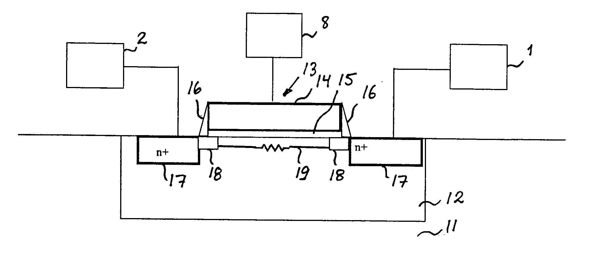
[0022] The present invention provides a device for ESD protection of a circuit of a semiconductor device comprising a field effect, preferably MOS, transistor based varistor with gate, source and drain regions, wherein one of the source and drain regions is connected to an input / output pad of the semiconductor device, and the other one of said source and drain regions is connected to an input / output terminal of the circuit. The device for ESD protection comprises a biasing circuit which is connected to the gate region of the field effect transistor based varistor to create an accumulation region there below at normal operating voltages of the semiconductor device to provide a very low series resistance.
[0025] The present invention thus provide for a different type of varistor with larger resistance ratio than the varistors-based prior art device since the ESD protection level is kept unchanged, while the series resistance at normal operating voltages is decreased.

Problems solved by technology

Integrated electrostatic discharges may damage electronic devices, particularly electronic semiconductor devices fabricated on insulating or semi-insulating substrates, such as integrated circuits.
For high frequency applications at gigahertz frequencies, however, the mentioned resistor creates several problems.
Furthermore, the resistance itself creates noise, which is deleterious in low noise applications.
While a prior art varistor solution as disclosed in WO03 / 021737 may provide an increase in the resistance of the varistor of four times when the voltage is increased from 0.5 to 7 V, and may have a capacitance as low as 70 fF, thereby fulfilling high frequency circuit requirements, the series resistance at normal operating voltages may be too high.
One manner to reduce the series resistance is to increase the size of the varistor, but then the parasitic capacitance will increase in turn, which is deleterious for high frequency circuits.

Method used


Image

  • Device for ESD protection of an integrated circuit
  • Device for ESD protection of an integrated circuit
  • Device for ESD protection of an integrated circuit

Examples


Embodiment Construction

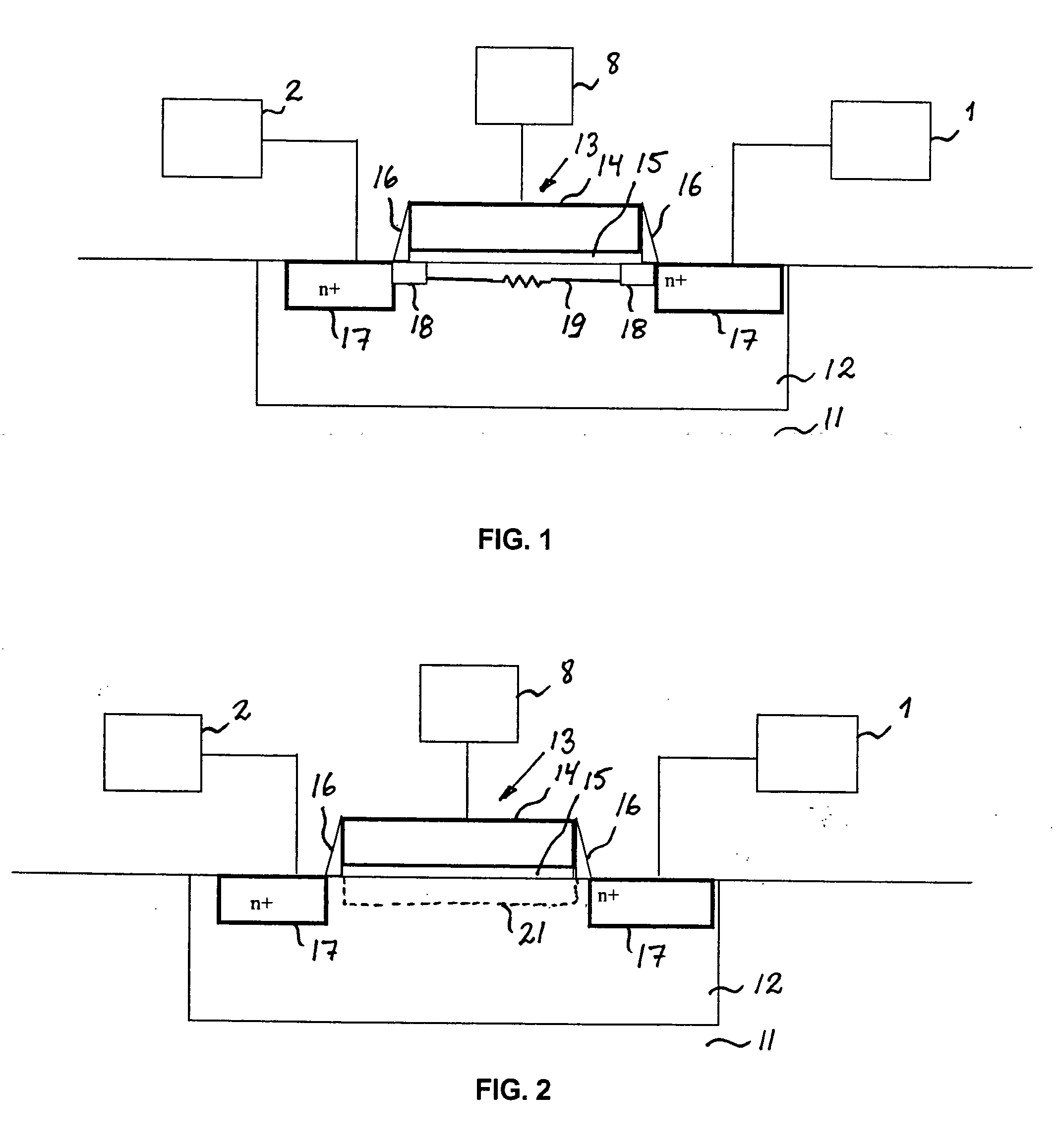
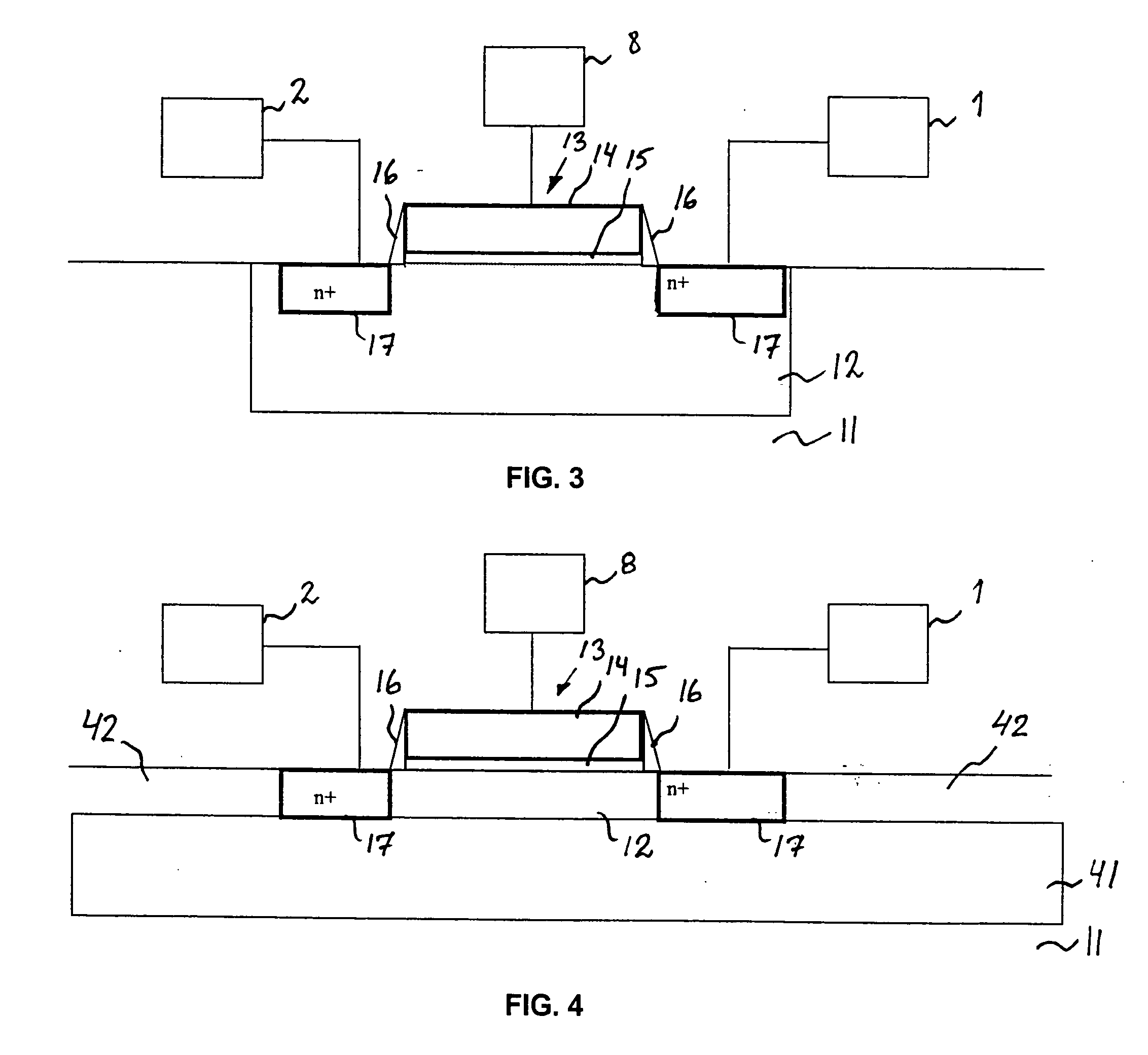
[0032] A monolithically integrated ESD protection device according to a preferred embodiment of the present invention is schematically shown in FIG. 1. The device includes a lateral field effect transistor structure, such as a MOS transistor structure, as being illustrated in a highly enlarged cross-sectional view, and a high impedance biasing circuit 8 as being schematically indicated. The MOS transistor structure operates as a varistor for current limitation purposes.

[0033] The ESD protection device is interconnected between a schematically illustrated input / output terminal of a high frequency or radio frequency MOS circuit 1, e.g. a receiver or driver circuit, and a likewise schematically illustrated input / output bonding pad 2. The semiconductor device comprising the MOS circuit 1, the ESD protection device, and the bonding pad 2 is in this embodiment preferably an integrated bulk substrate based device.

[0034] The lateral MOS transistor based varistor structure is formed in a p...


PUM


Abstract

A device for ESD (electrostatic discharge) protection of a circuit of a semiconductor device comprises a field effect transistor based varistor with gate, source and drain regions, wherein one of the source and drain regions is connected to an input / output pad of the semiconductor device, and the other one of the source and drain regions is connected to an input / output terminal of the circuit. A biasing circuit is connected to the gate region of the varistor to create an accumulation region below the gate of the varistor at normal operating voltages of said semiconductor device. The semiconductor device is preferably an integrated device on a single substrate.

Description

CROSS-REFERENCE TO RELATED APPLICATION [0001] This application claims priority from European Patent Application No. 04012772.2, which was filed on May 28, 2004, and is incorporated herein by reference in its entirety. BACKGROUND OF THE INVENTION [0002] 1. Field of the Invention [0003] The present invention generally relates to the field of integrated circuit technology, and more specifically the invention relates to a monolithically integrated device for ESD (electrostatic discharge) protection of an integrated circuit. [0004] 2. Description of Prior Art [0005] Integrated electrostatic discharges may damage electronic devices, particularly electronic semiconductor devices fabricated on insulating or semi-insulating substrates, such as integrated circuits. Devices for protecting against ESD are conventionally incorporated in the input / output paths of most semiconductor devices in order to shunt excessive charge away from the sensitive circuits of the semiconductor devices. [0006] Sem...

Claims


Application Information

Patent Timeline
Patent Type & Authority Applications(United States)
IPC IPC(8): H02H9/00H01L27/02
CPCH01L27/0288
Inventor LITWIN, ANDREJPETTERSSON, OLA
Owner INFINEON TECH AG
Learn More