Magnetoresistive element and magnetic memory

a magnetic memory and magnetoresistive element technology, applied in the field of magnetoresistive elements and magnetic memory, can solve the problems of increasing the size of the current magnetic field required for recording information reducing the current flowing through the interconnect, and difficult to supply a sufficient current magnetic field to the mtj elemen

Active Publication Date: 2009-10-01
KIOXIA CORP
View PDF5 Cites 65 Cited by
  • Summary
  • Abstract
  • Description
  • Claims
  • Application Information

AI Technical Summary

Problems solved by technology

With the advance in scale reduction, a current flowing through the interconnect decreases; for this reason, it is difficult to supply a sufficient current magnetic field to the MTJ element.
In addition, the size of the current magnetic field required for recording information to the MTJ element increases resulting from the scale reduction of the MTJ element.

Method used


Image

  • Magnetoresistive element and magnetic memory
  • Magnetoresistive element and magnetic memory
  • Magnetoresistive element and magnetic memory

Examples


first embodiment

[1] The Structure of MTJ Element

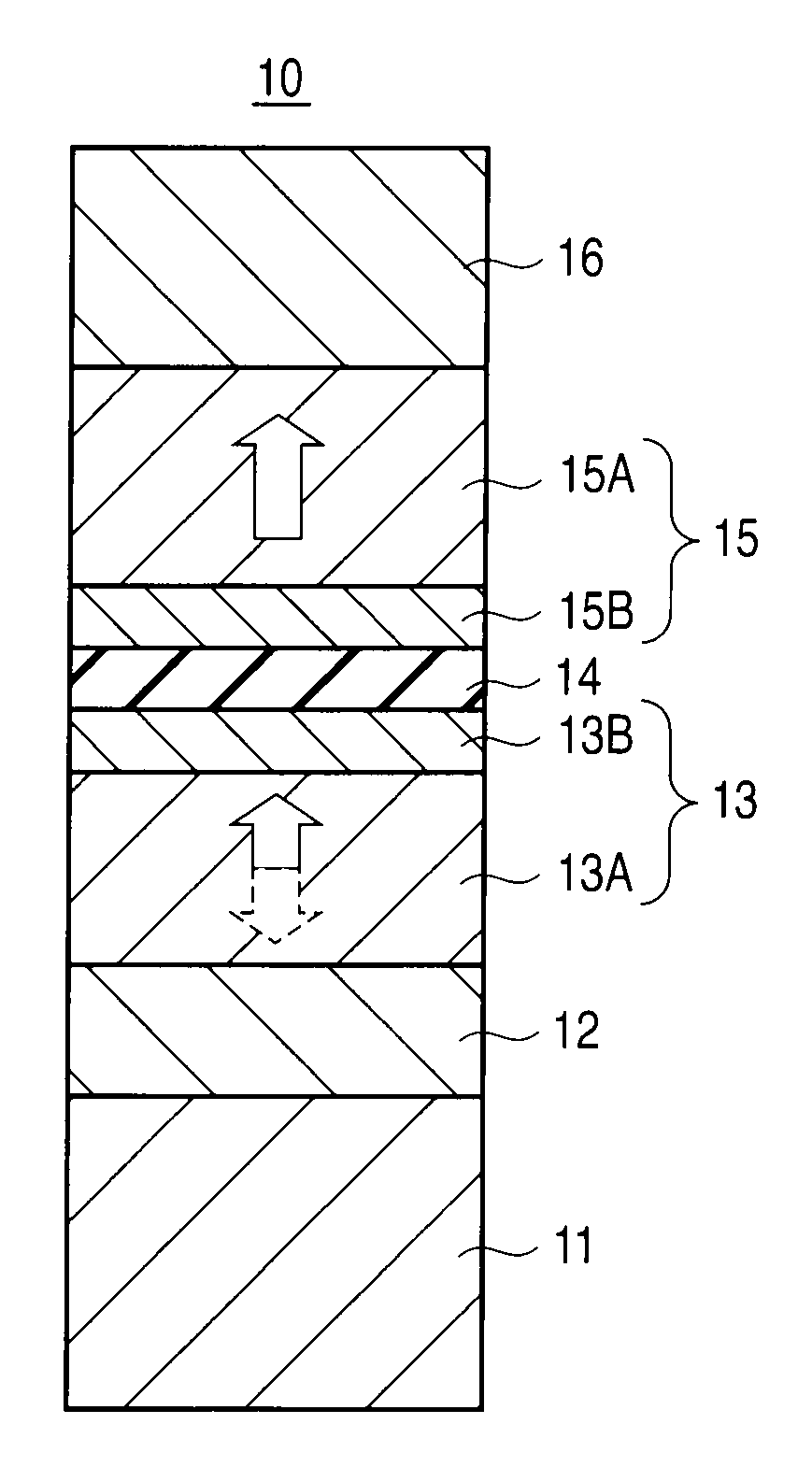
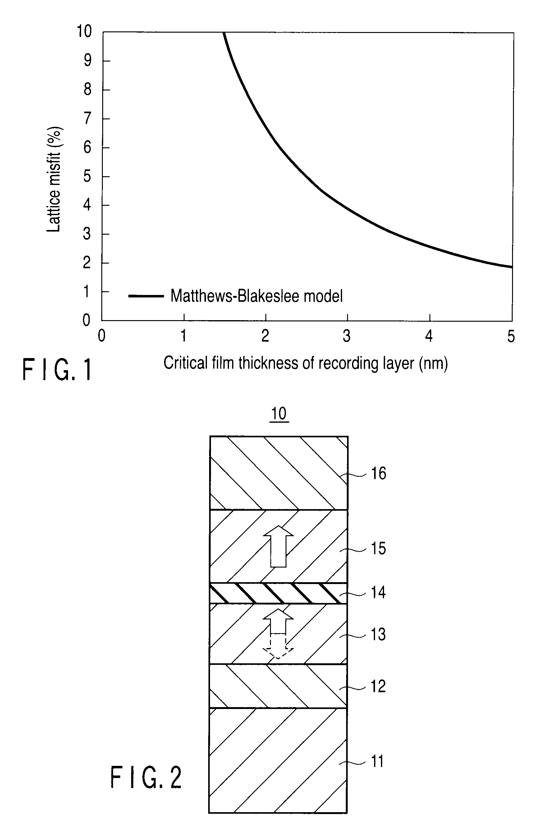
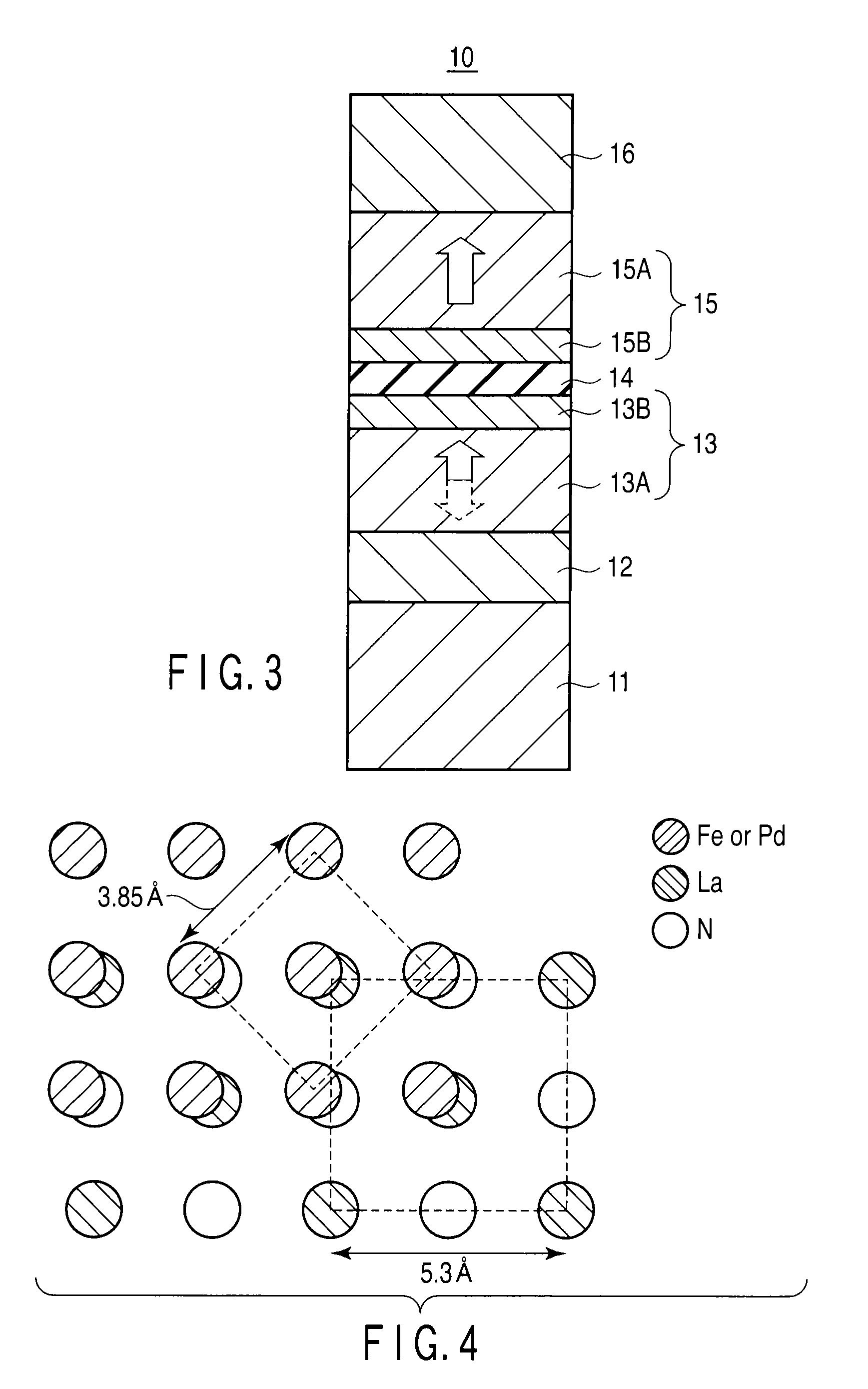
[0052]FIG. 2 is a cross-sectional view showing the structure of an MTJ element according to a first embodiment of the present invention. In FIG. 2, arrows denote the magnetization directions. According to this embodiment, an MTJ element 10 having a single pinned layer structure (i.e., structure in which one recording layer and one reference layer are stacked via a non-magnetic layer) will be described below as an example.

[0053]The MTJ element 10 has a stacked structure having the following layers successively stacked. The layers are a crystal orientation underlying layer 12, a recording layer (also called a free layer) 13, a tunnel barrier layer (non-magnetic layer) 14 and a reference layer (also called a pinning layer). Further, the bottom surface of the crystal orientation underlying layer 12 is provided with a bottom electrode 11, and the upper surface of the reference layer 15 is provided with a top electrode 16. For example, tantalum (Ta) is used...

second embodiment

[0104]According to a second embodiment, a magnetic-field adjusting layer 18 is newly added, and thereby, this serves to reduce a magnetic field leaking from the reference layer 15. In this way, the shift of switching magnetic field of the reference layer 13 resulting from the leaked magnetic field is reduced or controlled.

[0105]FIG. 6 is a cross-sectional view showing the structure of an MTJ element according to a second embodiment of the present invention. The structure from the bottom electrode 11 to the reference layer 15 is the same as the first embodiment.

[0106]A non-magnetic layer 17, a magnetic-field adjusting layer 18 and a top electrode 16 are successively stacked on a reference layer 15. The magnetic-field adjusting layer 18 has an effect of reducing a magnetic field leaking from the reference layer 15. The layer 18 is further used for adjusting a shift of a switching magnetic field of the recording layer 13 due to the leaked magnetic field.

[0107]The non-magnetic layer 17 ...

third embodiment

[0114]The third embodiment relates to the configuration of an MRAM configured using the MTJ element shown in the first or second embodiment.

[0115]FIG. 8 is a circuit diagram showing the configuration of an MRAM according to a third embodiment of the present invention. The MRAM includes a memory cell array 50 having a plurality of memory cells MC matrix-like arrayed. The memory array 50 is provided with a plurality of bit lines BL, / BL each extending in the column direction. The memory cell array 50 is further provided with a plurality of word lines WL each extending in the row direction.

[0116]The crossing portion of the bit line BL and the word line WL is provided with a memory cell MC. Each memory cell MC includes an MTJ element 10 and a select transistor 51 comprising an N-channel MOS transistor. One terminal of the MTJ element 10 is connected to the bit line BL. The other terminal of the MTJ element 10 is connected to a drain terminal of the select transistor 51. The gate termina...


PUM


Abstract

A magnetoresistive element includes an underlying layer having a cubic or tetragonal crystal structure oriented in a (001) plane, a first magnetic layer provided on the underlying layer, having perpendicular magnetic anisotropy, and having an fct structure oriented in a (001) plane, a non-magnetic layer provided on the first magnetic layer, and a second magnetic layer provided on the non-magnetic layer, and having perpendicular magnetic anisotropy. An in-plane lattice constant a1 of the underlying layer and an in-plane lattice constant a2 of the first magnetic layer satisfy the following equation in which b is a magnitude of Burgers vector of the first magnetic layer, ν is an elastic modulus of the first magnetic layer, and hc is a thickness of the first magnetic layer.
|√{square root over (2)}a1/2−a2|/a2<b×{ln (hc/b)+1}/{2π×hc×(1+ν)}

Description

CROSS-REFERENCE TO RELATED APPLICATIONS[0001]This application is based upon and claims the benefit of priority from prior Japanese Patent Application No. 2008-084938, filed Mar. 27, 2008, the entire contents of which are incorporated herein by reference.BACKGROUND OF THE INVENTION[0002]1. Field of the Invention[0003]The present invention relates to a magnetoresistive element and a magnetic memory. For example, the present invention relates to a magnetoresistive element which can store information by bidirectionally supplying a current thereto.[0004]2. Description of the Related Art[0005]A magnetic random access memory (MRAM) using a ferromagnetic material is anticipated as a nonvolatile memory having non-volatility, high-speed operation, large capacity and low power consumption. The MRAM includes a magnetic tunnel junction (MTJ) element using a tunneling magnetoresistive (TMR) effect as a memory element. The MRAM stores information according to the magnetization configuration of the...

Claims


Application Information

Patent Timeline
Patent Type & Authority Applications(United States)
IPC IPC(8): H01L29/82
CPCG11C11/16H01L43/08H01L27/222G11C11/161H10B61/00H10N50/10H10N50/01
Inventor KITAGAWA, EIJIYOSHIKAWA, MASATOSHINAGASE, TOSHIHIKODAIBOU, TADAOMINAGAMINE, MAKOTONISHIYAMA, KATSUYAKISHI, TATSUYAYODA, HIROAKI
Owner KIOXIA CORP
Why Eureka
Try Eureka