Semiconductor device having low dielectric constant film and manufacturing method thereof

a technology of dielectric constant film and semiconductor device, which is applied in the direction of semiconductor device, semiconductor/solid-state device details, electrical apparatus, etc., can solve the problems of low dielectric constant film, low mechanical strength of film, and increased capacity between the wiring lines, etc., to achieve the effect of improving the dielectric constan

Inactive Publication Date: 2009-10-01
TERAMIKROS INC
View PDF32 Cites 147 Cited by
  • Summary
  • Abstract
  • Description
  • Claims
  • Application Information

AI Technical Summary

Benefits of technology

[0010]It is therefore an object of this invention to provide a semiconductor device and a manufacturing method thereof enabling significant improvement of a low dielectric constant film that comes off.
[0013]According to this invention, a low dielectric constant film / wiring line stack structure which is made up of a stack of low dielectric constant films having a relative dielectric constant of 3.0 or less and wiring lines is provided in a region on the semiconductor substrate except for its peripheral part. The side surface of this low dielectric constant film / wiring line stack structure is covered with an insulating film, thereby enabling significant improvement of the low dielectric constant film that comes off. In this case, a lower protective film made of an organic resin is provided on the lower surface of the semiconductor substrate in order to protect the lower surface of the semiconductor substrate against cracks.

Problems solved by technology

In this case, if the distance between the wiring lines of the interlayer insulating film / wiring line stack structure is reduced due to miniaturization, the capacity between the wiring lines increases, and a signal transmitted through these wiring lines is more delayed.
However, the disadvantage of a semiconductor device having the above-described low dielectric constant film, in particular, the hollow porous low dielectric constant film is that the film is low in mechanical strength, susceptible to water, and apt to come off a foundation layer.

Method used


Image

  • Semiconductor device having low dielectric constant film and manufacturing method thereof
  • Semiconductor device having low dielectric constant film and manufacturing method thereof
  • Semiconductor device having low dielectric constant film and manufacturing method thereof

Examples


first embodiment

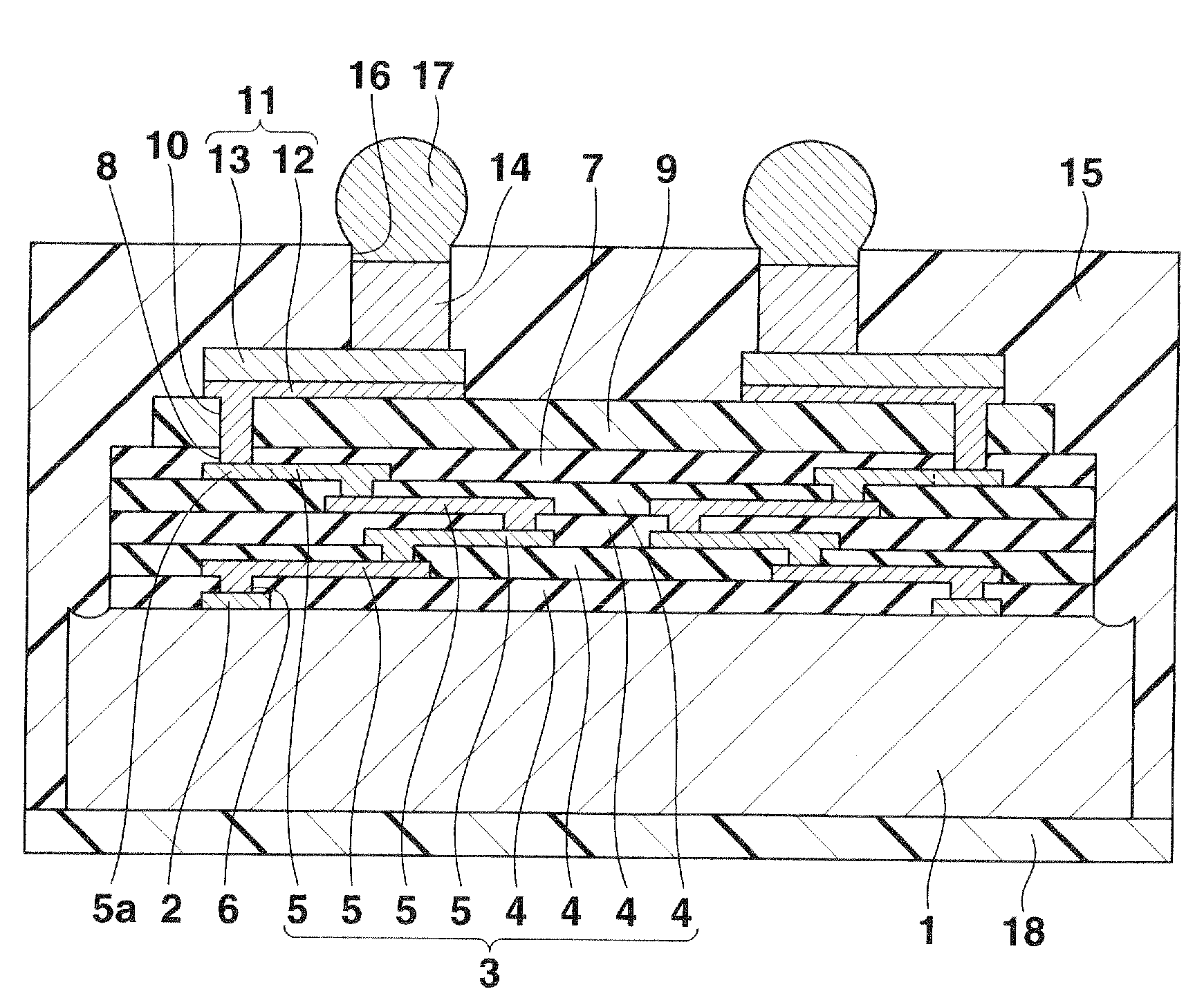
[0045]FIG. 1 shows a sectional view of a semiconductor device as a first embodiment of this invention. This semiconductor device comprises a silicon substrate (semiconductor substrate) 1. An integrated circuit having predetermined functions, in particular, elements (not shown) such as a transistor, a diode, a resistor and a condenser is provided on the upper surface of the silicon substrate 1. Connection pads 2 made of, for example, an aluminum-based metal and connected to the elements of the integrated circuit are provided in the peripheral parts of the upper surface of the silicon substrate 1. Although two connection pads 2 are only shown, a large number of connection pads 2 are actually provided on the upper surface of the semiconductor substrate.

[0046]A low dielectric constant film / wiring line stack structure 3 for connecting the elements of the integrated circuit is provided on the upper surface of the silicon substrate 1 except for a peripheral part outside the connection pads...

second embodiment

[0071]FIG. 13 shows a sectional view of a semiconductor device as a second embodiment of this invention. This semiconductor device is different from the semiconductor device shown in FIG. 1 in that the depth of a second trench 26 is smaller than that shown in FIG. 4. Therefore, the remainder of a silicon substrate 1 is formed as a projection 31 in the lower part of the peripheral side surface of the silicon substrate 1 between the lower surface of the silicon substrate 1 and the second trench 26. The side surface of this projection 31 is exposed to the outside, and the exposed side surface of this projection 31 is flush with the side surface of a sealing film 15. Further, a lower protective film 18 formed on the lower surface of the silicon substrate 1 covers the lower surface of the projection 31.

[0072]Next, one example of a method of manufacturing this semiconductor device is described. In this case, after the step shown in FIG. 3, a dicing blade 25 is used to cut a semiconductor ...

third embodiment

[0078]FIG. 18 shows a sectional view of a semiconductor device as a third embodiment of this invention. This semiconductor device is different from the semiconductor device shown in FIG. 13 in that a straight third trench 32 which exposes a sealing film 15 in the lower peripheral part of the lower surface of a silicon substrate 1 including a projection 31 is formed in order to remove the projection 31 and in that a lower protective film 18 is provided in the third trench 32.

[0079]Next, one example of a method of manufacturing this semiconductor device is described. In this case, after the step shown in FIG. 15, a dicing blade 33 is prepared as shown in FIG. 19. The dicing blade 33 is made of a disk-shaped whetstone. The section of its edge is substantially U-shaped. The thickness of the dicing blade 33 is greater than the width of a second trench 26. This dicing blade 33 is used to grind the lower side of a semiconductor wafer 21 including a projection forming portion 31a shown in F...


PUM


Abstract

A low dielectric constant film / wiring line stack structure made up of a stack of low dielectric constant films and wiring lines is provided in a region on the upper surface of the semiconductor substrate except for the peripheral part of this surface. The peripheral side surface of the low dielectric constant film / wiring line stack structure is covered with a sealing film. This provides a structure in which the low dielectric constant films do not easily come off. In this case, a lower protective film is provided on the lower surface of a silicon substrate to protect this lower surface against cracks.

Description

CROSS-REFERENCE TO RELATED APPLICATIONS[0001]This application is based upon and claims the benefit of priority from prior Japanese Patent Applications No. 2008-089674, filed Mar. 31, 2008; and No. 2008-224341, filed Sep. 2, 2008, the entire contents of both of which are incorporated herein by reference.BACKGROUND OF THE INVENTION[0002]1. Field of the Invention[0003]This invention relates to a semiconductor device having a low dielectric constant film and a manufacturing method thereof.[0004]2. Description of the Related Art[0005]A chip size package (CSP) having about the same size and dimensions as a semiconductor substrate is known as a semiconductor device mounted on small electronic equipment such as portable electronic equipment. A CSP which has been packaged in a wafer state and diced into semiconductor devices is called a wafer level package (WLP).[0006]Jpn. Pat. Appln. KOKAI Publication No. 2004-349461 has disclosed a semiconductor device, and this semiconductor device compri...

Claims


Application Information

Patent Timeline
Patent Type & Authority Applications(United States)
IPC IPC(8): H01L23/488H01L21/762
CPCH01L21/561H01L2224/0401H01L23/3114H01L23/3135H01L24/11H01L24/12H01L2221/6834H01L2221/68372H01L2221/68377H01L2224/03H01L2224/16H01L2224/274H01L2924/10157H01L2924/10158H01L2924/12044H01L2924/14H01L2924/19041H01L2924/30105H01L2924/01019H01L24/27H01L21/6835H01L2924/01029H01L2924/3512H01L2924/00H01L2224/11H01L2224/94H01L2224/04105H01L2224/12105H01L23/485H01L23/488
Inventor KOROKU, TAISUKEWAKABAYASHI, TAKESHIOKADA, OSAMUKUWABARA, OSAMUSHIOTA, JUNJIFUJII, NOBUMITSU
Owner TERAMIKROS INC
Why Eureka
Try Eureka