Organic Electroluminescence Element, Method for Manufacturing the Same and Organic Electroluminescence Display Device

Inactive Publication Date: 2009-10-01
TOPPAN PRINTING CO LTD
View PDF2 Cites 41 Cited by
  • Summary
  • Abstract
  • Description
  • Claims
  • Application Information

AI Technical Summary

Problems solved by technology

Current is difficult to flow.
A sufficient light emitting luminance can not be obtained.
In addition, hol

Method used


Image

  • Organic Electroluminescence Element, Method for Manufacturing the Same and Organic Electroluminescence Display Device
  • Organic Electroluminescence Element, Method for Manufacturing the Same and Organic Electroluminescence Display Device
  • Organic Electroluminescence Element, Method for Manufacturing the Same and Organic Electroluminescence Display Device

Examples


example 1

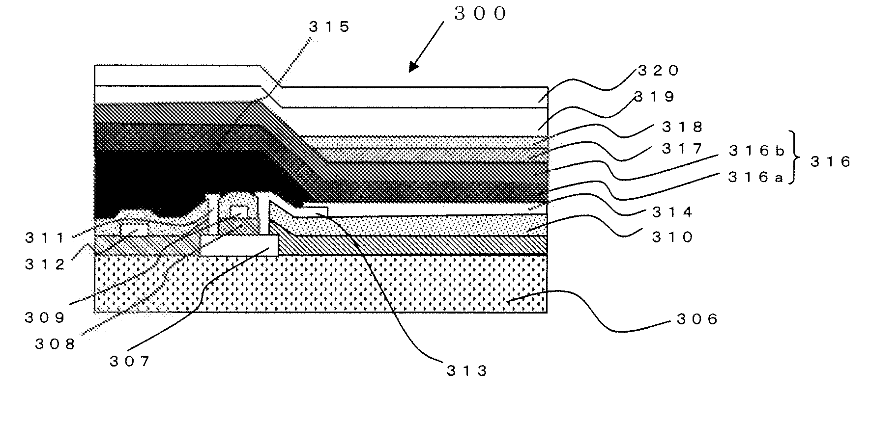
[0210]As shown in FIG. 5, an active matrix substrate 306 with a thickness of 0.7 mm was used. The active matrix substrate 306 had a thin film transistor formed on a substrate 306, the transistor functioning as a switching element, and a pixel electrode 314 electrically connected to a source electrode 313, the pixel electrode 314 formed above the thin film transistor. As for a substrate 306, the diagonal size was 5 inches and the number of pixels was 320×240.

[0211]A partition wall 315 was formed so that its shape allowed it to cover an end of the pixel electrode 314 provided on this substrate 306 and to section pixels. The partition wall 315 was formed by the following processes: a positive resist (ZWD6216-6: a product of ZEON CORPORATION) was formed on the entire surface of the substrate 306 by a spin coater so that the thickness of the resist was 2 μm; and the partition wall having a width of 40 μm was formed by patterning using a photolithography method. In this way, the pixel reg...

example 2

[0218]A sample was manufactured by the same way as Example 1, thereby sample with a pixel electrode 314 was prepared. Next, as a hole a transport layer, a pattern of a crystal containing layer 316a of molybdenum oxide of 100 nm thickness was formed by both a reactive sputtering method and a shadow mask method while a substrate 6 was heated to 150 degrees Celsius. The sample was manufactured by the same way as Example 1 except for the above. The obtained active matrix drive type organic EL display device 300 was driven. At initial time, there was not uneven luminance and a nonlighting area, and a light emitting is even and excellent. In addition, luminance was 8000 cd / m2 at 6 V, and half life of luminance in the case of initial luminance of 8000 cd / M2 was 1200 hrs. That is, the display characteristic was excellent (a high light emitting efficiency, a high light emitting luminance and a long life time). In addition, the current value rapidly increased at 1400 hrs.

example 3

[0219]A sample was manufactured by the same way as Example 1, thereby a sample with a pixel electrode 314 was prepared. Next, as a hole transport layer, a pattern of a crystal containing layer 316a of molybdenum oxide of 80 nm thickness was formed by both a reactive sputtering method and a shadow mask method while a substrate 6 was heated to 300 degrees Celsius. In a condition where a substrate 6 is cooled to a room temperature, a pattern of an amorphous layer 316b of 20 nm thickness was formed by a reactive sputtering method and a shadow method. The sample was prepared by the same way as Example 1 except for the above.

[0220]The obtained active matrix drive type organic EL display device 300 was driven. At initial time, there was not uneven luminance and a nonlighting area, and a light emitting is even and excellent. In addition, luminance was 8000 cd / m2 at 8 V, and half life of luminance in the case of initial luminance of 8000 cd / m2 was 1500 hrs. That is, the display characteristi...


PUM


Abstract

One embodiment of the present invention is an organic electroluminescence element including an anode which is a hole injection electrode; a cathode which is an electron injection electrode, the cathode facing the anode; an organic light emitting layer between the anode and the cathode, the organic light emitting layer including a molybdenum oxide layer, the molybdenum oxide layer including a crystal molybdenum oxide and an amorphous molybdenum oxide, and the crystal molybdenum oxide and the amorphous molybdenum oxide being mixed or stacked.

Description

CROSS REFERENCE[0001]This application is based upon and claims the benefit of priority from the prior Japanese Patent Application No. 2008-081351, filed on Mar. 26, 2008, the entire contents of which are incorporated herein by reference.BACKGROUND OF THE INVENTION[0002]1. Field of the Invention[0003]The present invention is related to an organic electroluminescence element, a method for manufacturing the element and an organic electroluminescence display device. In particular, the present invention is related to an organic electroluminescence element, a method for manufacturing the element and an organic electroluminescence display device, in which the element and the display utilize electroluminescence (EL) phenomenon of an organic thin film.[0004]2. Description of the Related Art[0005]An organic EL element has an organic light emitting layer presenting an electroluminescent phenomenon between an anode and a cathode. When a voltage is applied between the electrodes, a hole and elec...

Claims


Application Information

Patent Timeline
IPC IPC(8): H01J1/63B05D5/12
CPCH01L51/5048H05B33/22H01L2251/558H01L51/5088H10K50/14H10K50/17H10K2102/351
Inventor SHODA, RYOKITAZUME, EIICHIKANETA, SHINGO
Owner TOPPAN PRINTING CO LTD
Why Eureka
Try Eureka