
Process and apparatus for the production of collimated UV rays for photolithographic transfer

a technology of collimated uv rays and photolithographic transfer, which is applied in the direction of optics, circuit masks, instruments, etc., can solve the problems of large space requirements of optics and high cost, and achieve the effect of reducing the optical length of downstream optics

Inactive Publication Date: 2009-10-01
RADOVE
View PDF15 Cites 29 Cited by
  • Summary
  • Abstract
  • Description
  • Claims
  • Application Information

AI Technical Summary

Benefits of technology

[0006]The present invention provides an improved process and an apparatus for producing collimated UV radiation for exposing a photosensitive substrate on printed circuit boards. The process and apparatus of the present invention does not require the long optical paths of prior collimated UV radiation devices in the field. The present invention accomplishes the object of shortened optical length of the downstream optics by dividing the collimated UV radiation from an up-stream radiation source into a plurality of secondary radiation sources, and by distributing the UV radiation from the secondary source to uniformly radiate the target substrate by using a scanning slide.
[0008]In a preferred embodiment of the second technique, the UV LEDs are bonded or soldered directly on a heat sink. In this embodiment, it is also preferred that the heat sink material is cooled to an appropriate temperature, e.g., 6° C. using water cooling, in order to maximize the service life and to help stabilize the UV output radiation of the UV LEDs.
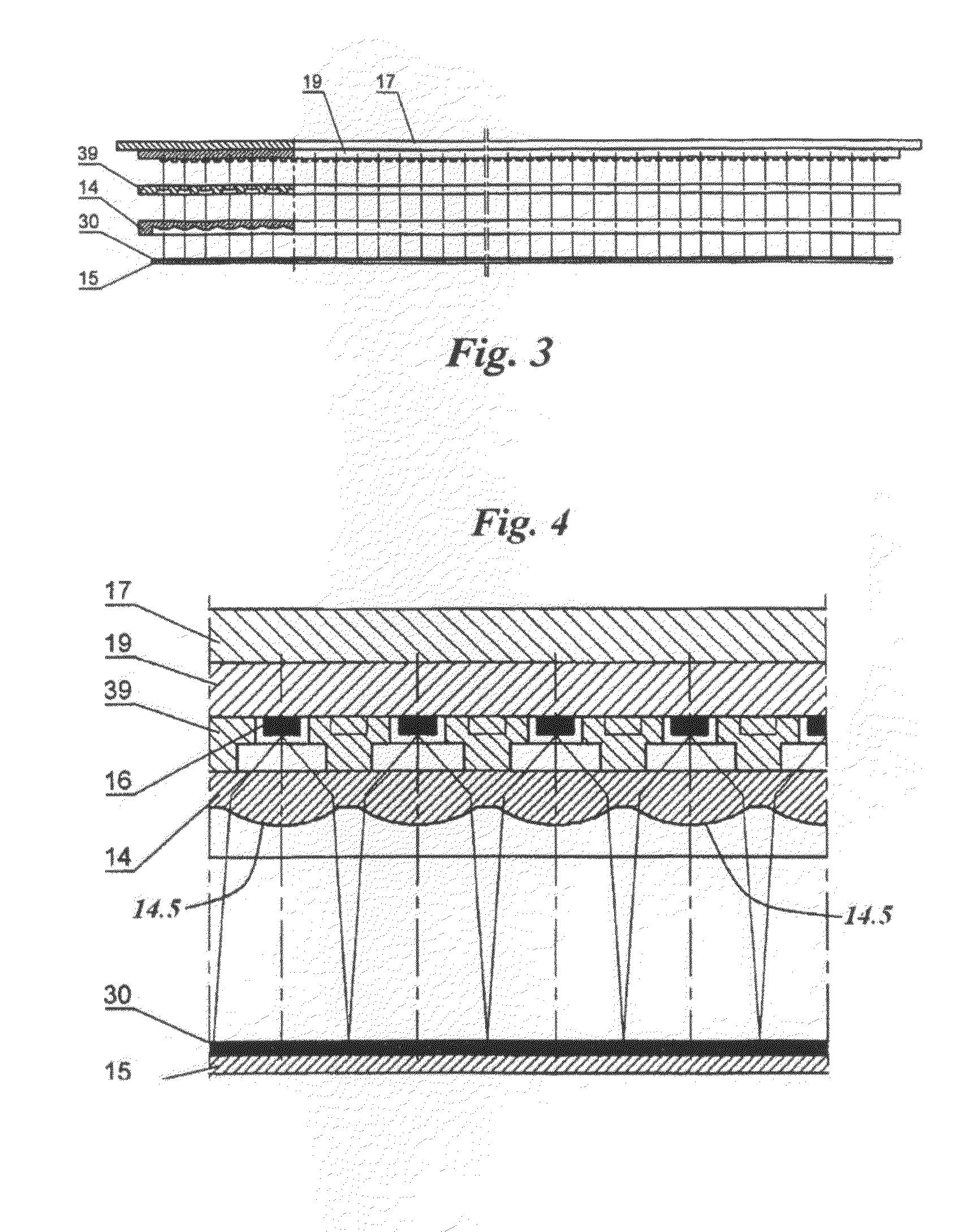
[0009]In the preferred embodiment, the UV LEDs and UV LED chip clusters are arranged as a square, and the square arrangement is rotated by 45° so that the diagonal of the chip clusters is parallel to the direction of scanning movement of the scanning slide. Given suitable magnification of the square radiation source by the collimation lenses, these are projected on the substrate rhomboidal subareas whose radiation densities add up optimally during scanning with the radiation densities of the rhomboidal subareas of adjacent LEDs and further yield good uniformity. Details of this process are described in the exemplary embodiments viewed with the aid of the drawings.
[0013]The uniformity of the exposure is an important variable for the functioning of the resist in the subsequent process steps: development / electroplating / etching. It is therefore advantageous to introduce the exposure energy into the substrate uniformly.
[0019]The invention supplies a process that produces from the measured data a program for the printed circuit board milling machine used to produce a milled part that can be used as aperture contour for improving the uniformity. The user is thus in the position of measuring his machine periodically (e.g., yearly) and himself producing the required calibrated aperture with a low outlay.
[0020]A further method improves the uniformity errors that are produced by an unsatisfactory stability of the scanning movement. US 2002 / 016 788 A1 describes a method of controlling the exposure energy / cm2 for the resist merely by varying the scanning speed. The resist / soldering sensitivities range from 10 mJ / cm2 to 500 mJ / cm2. Because of the wide span, it is not possible to adapt the exposure energy to the resist merely via the variation of the scanning speed. The present invention therefore uses constant speeds for which optimal PID parameters are respectively fixed for the purpose of motor control. The fine control and the further adaptation of the range are performed solely via control of the current to the LEDs. Only thus is it possible to have a resolution of 1% in the case of the energy density for all the resist / soldering resist exposures.

Problems solved by technology

These optics therefore have a large space requirement and are very expensive.

Method used


Image

  • Process and apparatus for the production of collimated UV rays for photolithographic transfer
  • Process and apparatus for the production of collimated UV rays for photolithographic transfer
  • Process and apparatus for the production of collimated UV rays for photolithographic transfer

Examples


Embodiment Construction

)

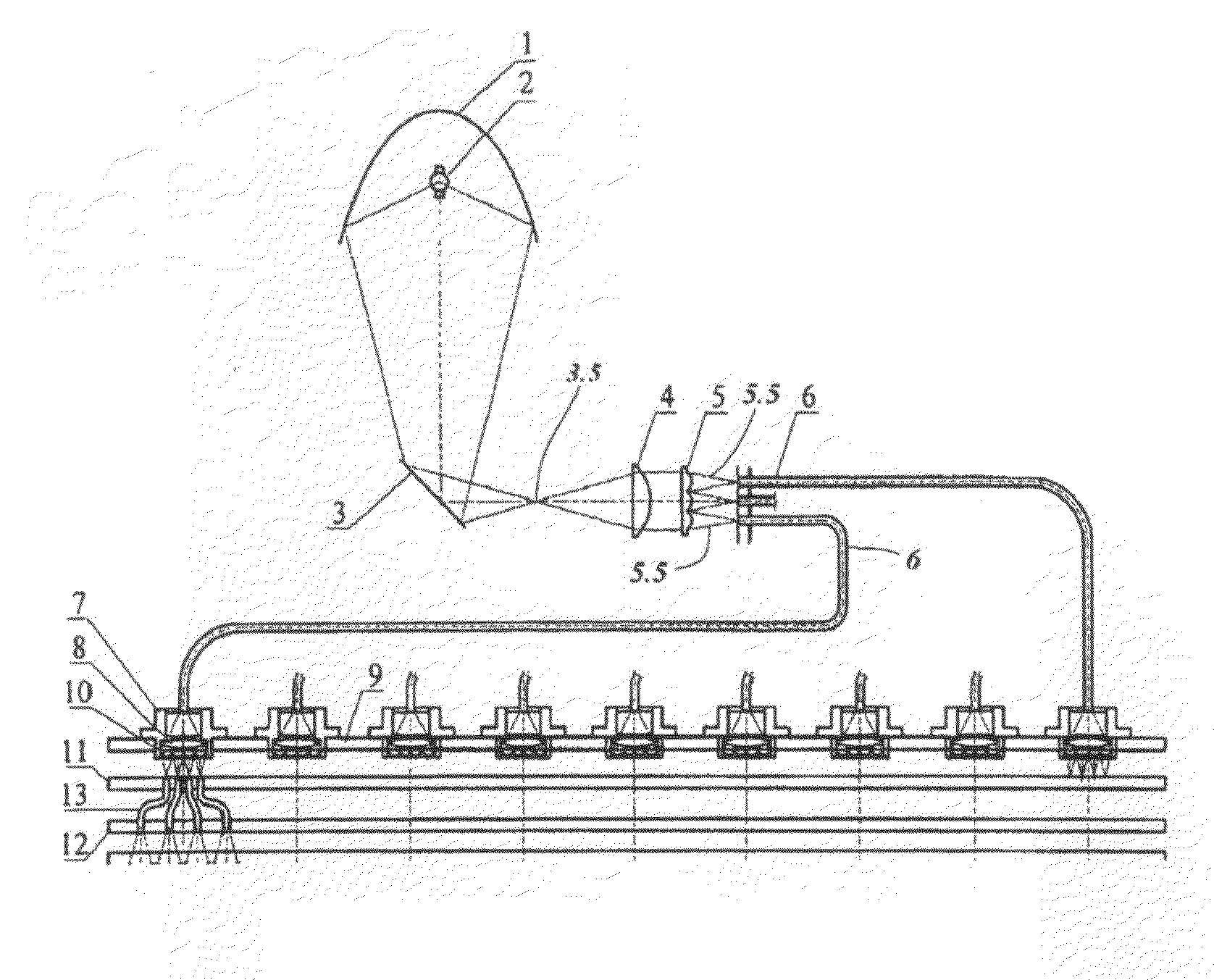
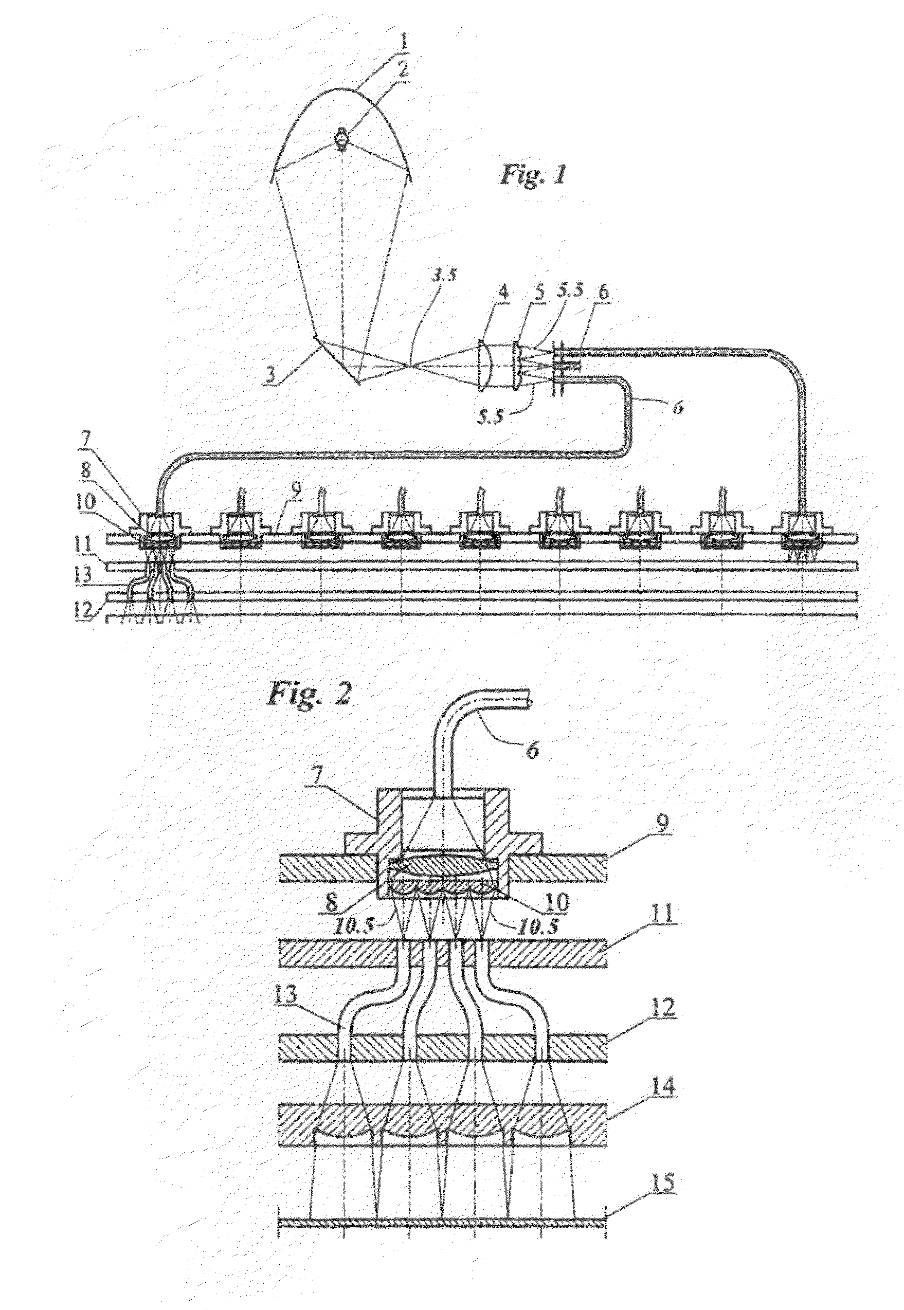
[0038]FIGS. 1, 2 show the UV collimation optics based on liquid light guides. In this embodiment, the UV radiation of a mercury short arc lamp (2) is concentrated at a focal point (3.5) with the aid of an ellipsoid (1). A cold light mirror (3) is disposed in front of the focal point (3.5) and deflects the beam (by 90° in the embodiment illustrated) toward a collimation lens (4). The collimation lens (4) concentrates the UV radiation onto a raster lens plate (5) that splits the beam into a plurality of split beams (5.5) and focuses the split beams (5.5) onto the entrance ports (6.5) of a multiliquid light guide (6).

[0039]The liquid light guides (6) transmit the UV radiation at low loss toward the base plate (9) of a scanning slide (50). Each liquid light guide (6) ends in a flange (7) that is fastened on the base plate (9). The component UV radiation beam of a liquid light guide (6) is concentrated with the aid of a 2nd collimation lens (8) onto a second raster lens plate (10). The ...


PUM


Abstract

The present invention provides an improved process and an apparatus for producing collimated UV radiation for exposing printed circuit boards. The process consists in shortening the optical length of the downstream optics by dividing the UV radiation over many radiation sources, and in distributing the UV radiation uniformly on the substrate by using a scanning slide.

Description

FIELD OF THE INVENTION[0001]The invention relates to a collimation optics for the photolithographic transfer of patterns onto substrates coated with a photosensitive polymer. More specifically, the present invention relates to collimated UV optics for photolithographic transfers onto printed circuit boards.BACKGROUND OF THE INVENTION[0002]Exposure systems with UV collimation optics are used for exposing printed circuit boards with conductor tracks<100μ.[0003]UV collimation optics are known in the field. See for example, the descriptions in EP 618 505, EP 807 505, EP 807 856, DE 41066 7311, and US 2002 / 016 7788 A1, the contents of which are incorporated herein by reference. The prior UV collimation optics collect the UV radiation of a mercury short arc lamp at the focus of an ellipsoidal mirror and expand this focus to a parabolic mirror via a collimation optics. The UV rays leave the parabolic mirror in a fashion that is collimated and perpendicular to the substrate.[0004]In the...

Claims


Application Information

Patent Timeline
IPC IPC(8): G03B27/54
CPCG03F7/70383H05K3/0082G03F7/70391
Inventor DOMANOWSKI, PIOTR
Owner RADOVE
Learn More