Adhesive Composition, Adhesive Sheet and Production Method of Semiconductor Device

Inactive Publication Date: 2009-10-01
LINTEC CORP
View PDF8 Cites 17 Cited by
  • Summary
  • Abstract
  • Description
  • Claims
  • Application Information

AI Technical Summary

Benefits of technology

[0055]In a production of a semiconductor device on which chips being reduced in a thickness is mounted, a strength necessary for pick-up in a pick-up step is reduced due to the adhesive sheet of t

Problems solved by technology

If the value of this is high, the chips may be broken or chipped when being picked up, which reduces the manufacturing yield of the chips.
In summ

Method used


Image

  • Adhesive Composition, Adhesive Sheet and Production Method of Semiconductor Device
  • Adhesive Composition, Adhesive Sheet and Production Method of Semiconductor Device
  • Adhesive Composition, Adhesive Sheet and Production Method of Semiconductor Device

Examples


examples

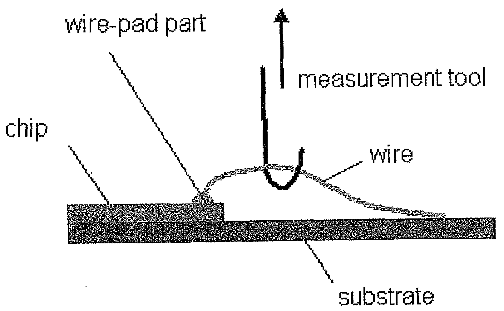
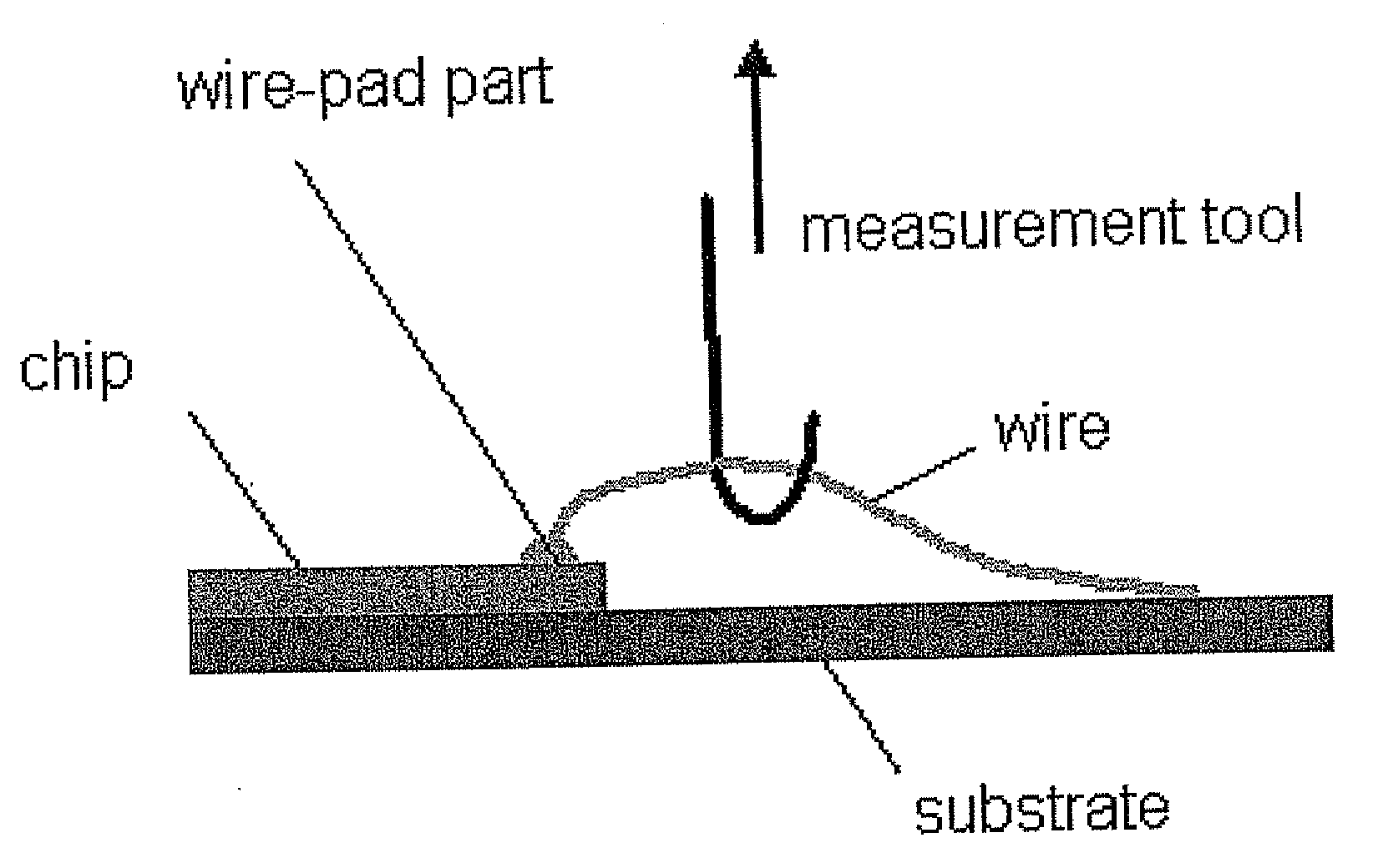
[0165]Hereinbelow, the present invention shall be explained with reference to examples, but the present invention shall not be restricted to these examples. In the following examples and comparative examples, “Picking-up Load Measurement”, “Picking-up test” and “Wire Pulling Test” were conducted as follows.

[Picking-Up Load Measurement]

[0166]Each of adhesive sheets of the examples and comparative examples was adhered on the back side of a 6-inch wafer (thickness: 350 μm, backside: #2000 ground), and the wafer was fixed to a ring frame (2-6-1 available from DISCO Corporation). The wafer was subjected to full cutting into 5 mm square chips using a dicing machine (DFD651 available from DISCO Corporation; dicing blade: 27HECC available from DISCO Corporation) under the following conditions. The feeding speed of the blade, the number of rotations and the cutting depth into the adhesive sheets were 50 mm / sec, 30,000 rpm and 50 μm, respectively.

[0167]The adhesive sheet was expanded over the...


PUM

PropertyMeasurementUnit
Kinematic viscosityaaaaaaaaaa
Forceaaaaaaaaaa
Forceaaaaaaaaaa

Abstract

The object of the present invention is to provide an adhesive composition that enables to produce conforming products with a high manufacturing yield and without breaking or chipping of the chips in the picking-up step and that enables to stably connect a wire without contaminating a wire pad part disposed at the circumference of a bonding surface during a wire bonding step that is performed after die bonding, even in the case of chips being reduced in a thickness.
The adhesive composition of the present invention comprises:
    • (A) an acrylic polymer;
    • (B) an epoxy resin;
    • (C) a thermosetting agent; and
    • (D) a silicone compound,
    • wherein the silicone compound (D) has one kind of reactive organic functional group and a kinematic viscosity within a specific range.

Description

BACKGROUND OF THE INVENTION[0001]1. Field of the Invention[0002]The present invention relates to an adhesive composition which is particularly suited for using at dicing step where chips are obtained from a semiconductor wafer and a step of die-bonding a chip on an organic substrate or a lead frame and the like, an adhesive sheet having an adhesive layer comprising the above adhesive composition and a production method of a semiconductor device using the above adhesive sheet.[0003]2. Description of the Related Art[0004]A semiconductor wafer of silicon, gallium arsenide or the like is produced in a large size, and this wafer is cut and separated (dicing) into small element pieces (chips) and then transferred to a die-bonding step which is a subsequent step. In this case, the semiconductor wafer is subjected to the respective steps of dicing, washing, drying, expanding and picking-up in the state that it is adhered advance on an adhesive sheet, and then it is transferred to a die-bond...

Claims


Application Information

Patent Timeline
IPC IPC(8): H01L21/50C08L83/04C09J7/20
CPCC08G77/26H01L2924/01028C08L83/00C09J7/02C09J133/08C09J163/00C09J2203/326C09J2433/00C09J2463/00H01L21/6835H01L23/296H01L24/27H01L24/29H01L24/31H01L24/45H01L24/48H01L24/83H01L24/85H01L2224/27436H01L2224/2919H01L2224/29191H01L2224/45015H01L2224/45144H01L2224/48091H01L2224/48227H01L2224/48465H01L2224/83191H01L2224/83855H01L2224/859H01L2924/01004H01L2924/01005H01L2924/01013H01L2924/01014H01L2924/0102H01L2924/01025H01L2924/01027H01L2924/01029H01L2924/01078H01L2924/01079H01L2924/01082H01L2924/07802H01L2924/09701H01L2924/12044H01L2924/14H01L2924/20752H01L2224/29H01L2224/45124H01L2924/01006H01L2924/01019H01L2924/01033H01L2924/014H01L2924/0665H01L2224/29101H01L2924/0132H01L2224/2929H01L2224/29386H01L2224/29388H01L2924/00013C08L33/00C08L2666/04C08L2666/02H01L2924/00014H01L2924/0715H01L2924/0635H01L2924/00H01L2924/05442H01L2924/05432H01L2924/04642H01L2924/0503H01L2924/3512H01L2224/29099H01L2224/29199H01L2224/29299H01L2924/181C09J7/20
Inventor ICHIKAWA, ISAOSAIKI, NAOYASHIZUHATA, HIRONORI
Owner LINTEC CORP
Why Eureka
Try Eureka