Sample inspection apparatus

a technology of sample inspection and sample, which is applied in the direction of material analysis using wave/particle radiation, instruments, nuclear engineering, etc., can solve the problems of difficult identification of faulty points, difficult to find such changes, and hardly appear the brightness between faulty points and normal points, so as to reduce the potential difference between samples and probes, reduce the acceleration voltage, and prevent damage

Active Publication Date: 2009-10-08
HITACHI HIGH-TECH CORP
View PDF2 Cites 14 Cited by
  • Summary
  • Abstract
  • Description
  • Claims
  • Application Information

AI Technical Summary

Benefits of technology

[0016]The surface of the sample may be charged, or there may be a potential difference between a probe and the sample surface. In such a case, an electric discharge phenomenon may occur between the probe and the sample at the moment of their contact. Thus, the probe or the sample may be damaged. A function is provided to automatically drop the optical conditions of the charged particles down to predetermined conditions when the probe is to be moved. For example, an acceleration voltage may be lowered. Alternatively, an emission current or a probe current may be lowered. In such a manner, the potential difference between the sample and the probe can be reduced so that the probe or the sample can be prevented from being damaged due to electric discharge or the like.
[0017]When a probe is to be moved, the probe may be electrically changed over to the ground level of the apparatus so as to restrain electric discharge or the like from occurring. Once the movement and the contact have been confirmed, electric connection of the probe is restored to its original connection, and the electro-optical conditions for irradiation of the sample with charged particles are also restored to their original conditions. When images are obtained continuously over a long time, a similar phenomenon may occur. When the optical conditions or the electric level of each probe is changed in the

Problems solved by technology

However, when a resistance component of a faulty point is low or when wiring to be inspected is complicated, a difference in brightness between the faulty point and a normal point hardly appears so that it is difficult to identify t

Method used


Image

  • Sample inspection apparatus
  • Sample inspection apparatus
  • Sample inspection apparatus

Examples


first embodiment

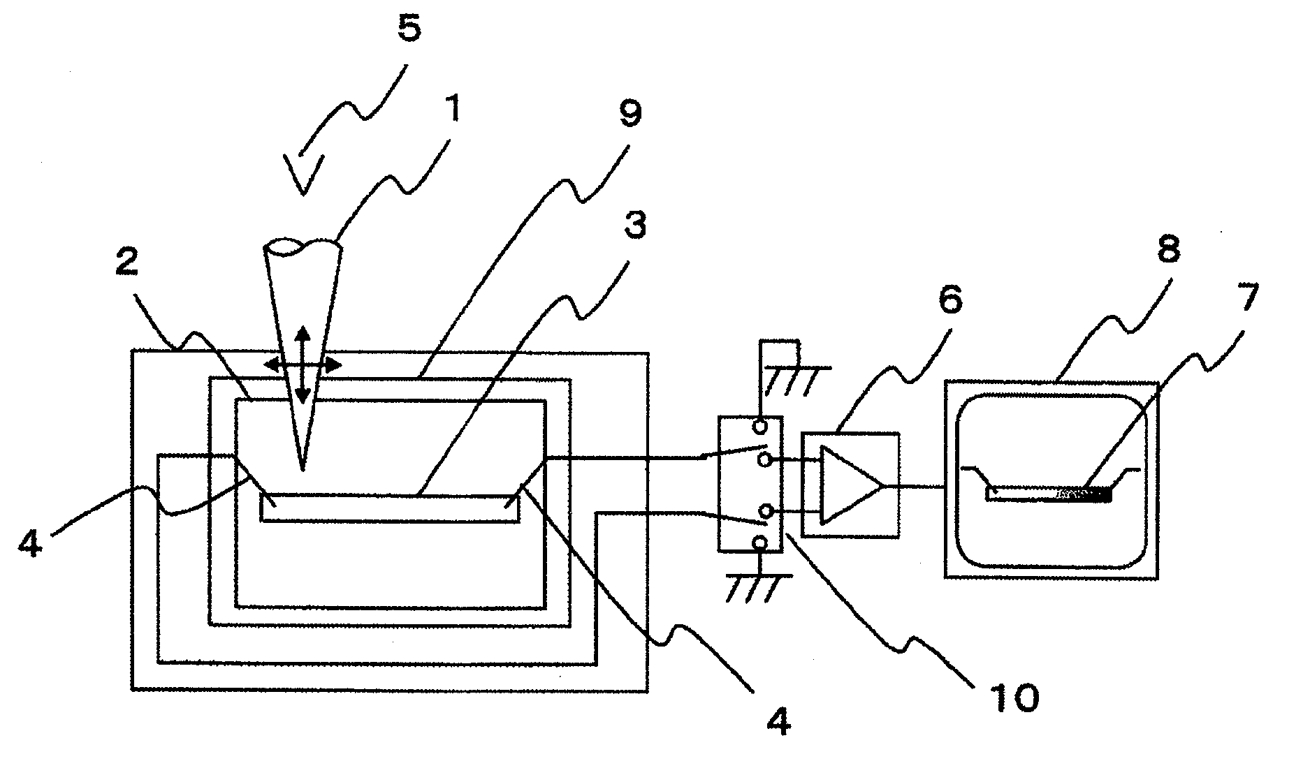
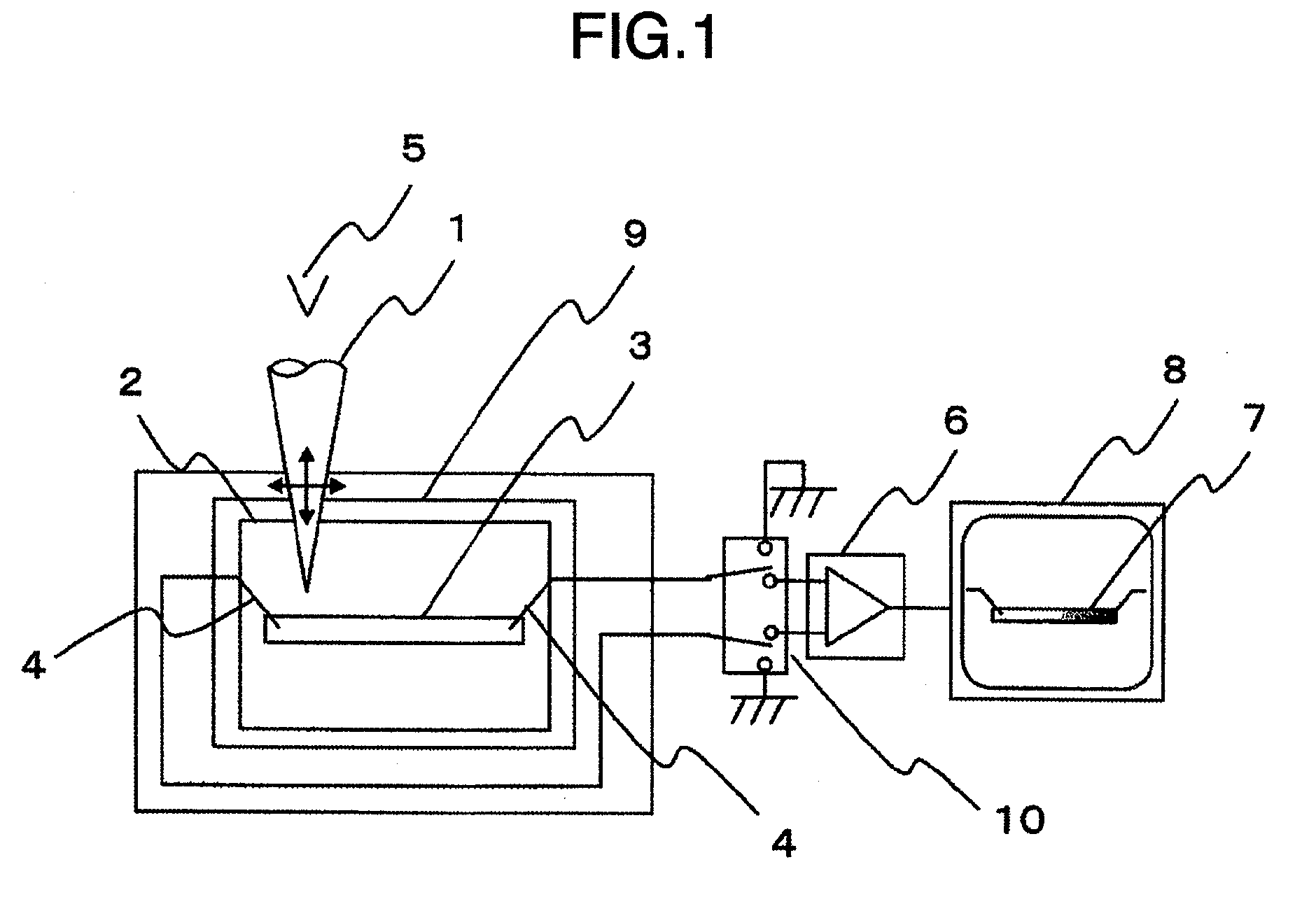
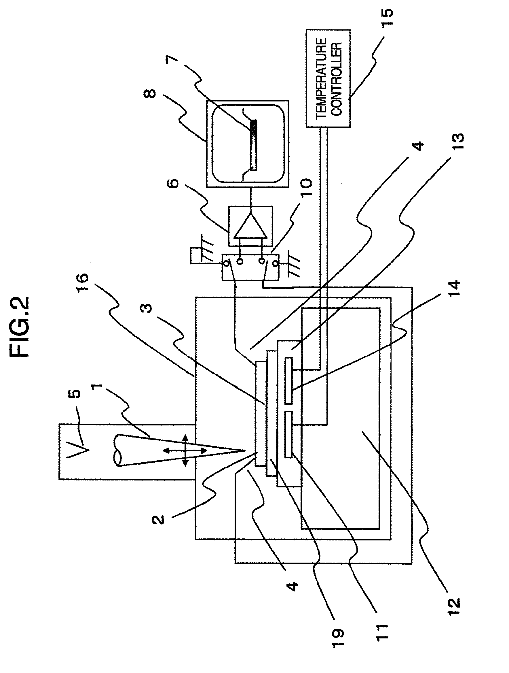
[0036]FIG. 1 is a schematic configuration diagram of a sample inspection apparatus to which an embodiment of the present invention is applied.

[0037]A sample 2 is irradiated with a primary electron beam 1. There is a wiring pattern 3 in the surface of the sample 2. Probes 4 are brought into contact with one side or opposite ends of the wiring pattern 3 or a pad thereof. In this state, the surface of the sample 2 including the wiring pattern 3 is scanned with the primary electron beam 1 by an electron beam source 5.

[0038]Of the radiated primary electron beam 1, electrons flowing into the wiring pattern 3 are detected as a current by the probes 4. The detected current is inputted to an amplifier 6 so as to be amplified by the amplifier 6. The amplifier 6 generates and outputs a signal in accordance with the inputted signal. The outputted signal is synchronized with the scan with the primary electron beam 1 and displayed on a display portion 8 as an absorbed electron current image 7.

[00...

second embodiment

[0042]FIGS. 3A and 3B show expressions of weighted addition and subtraction of two absorbed electron current images. Two absorbed electron current images are added / subtracted with weighting constants w and g. The two images may be images obtained with the temperature being changed. Alternatively, the two images may be absorbed electron current images obtained with the electro-optical conditions being changed, or absorbed electron current images obtained with the contact positions of the probes being changed.

[0043]FIGS. 4A and 4B show expressions in the case where the number of images in weighted addition and subtraction is increased to three or more while it is 2 in FIGS. 3A and 3B. FIGS. 4A and 4B show examples of images obtained in different temperatures when K=2.

third embodiment

[0044]FIG. 5 shows an explanatory example of a simple difference between two images obtained in different sample temperatures. Based on the obtained differential image, only a portion whose contrast has changed in accordance with the temperature change is emphasized.

[0045]Here, weighting coefficients may be determined so that pixel values in one and the same position in an image at a sample temperature A° C. and an image at a sample temperature B° C. can be equalized to each other.

[0046]Even if the position corresponds to a faulty position, pixel values in the other site than the faulty position will remain in an image obtained by weighted difference. Consequently, the faulty position will be emphasized.

[0047]FIG. 6 shows an example where in order to identify a short-circuit point in parallel wires, probes are brought into contact therewith at a plurality of points so as to obtain a plurality of absorbed electron current images concurrently, and weighted subtraction is performed on ...


PUM


Abstract

A sample inspection apparatus in which a fault in a semiconductor sample can be measured and analyzed efficiently. A plurality of probes are brought into contact with the sample. The sample is irradiated with an electron beam while a current flowing through the probes is measured. Signals from at least two probes are supplied to an image processing unit so as to form an absorbed electron current image. A difference between images obtained in accordance with a temperature change of the sample is obtained. A faulty point is identified from the difference between the images.

Description

BACKGROUND OF THE INVENTION[0001]The present invention relates to a sample inspection apparatus for analyzing a semiconductor sample or the like, and a method for producing an absorbed electron current image using the sample inspection apparatus. Particularly, it relates to a technique for specifying an electrically faulty point in wiring of a semiconductor sample or the like.[0002]With development of finer devices, it has been difficult to specify a faulty point in a semiconductor sample having a circuit formed in the semiconductor surface, and it has taken enormous time to analyze the fault. For this reason, analyzers such as OBIRCH (Optical Beam Induced Resistance Change) or EB testers are used currently.[0003]In the field of fault analysis in semiconductor samples, attention has been recently paid to wiring fault analyzing techniques in which the surface of a semiconductor sample is irradiated with an electron beam and a current absorbed from the wiring or a secondary signal emi...

Claims


Application Information

Patent Timeline
IPC IPC(8): G01N23/00
CPCH01J37/28H01J2237/24495H01J2237/2803H01J2237/24592H01J2237/24564
Inventor NARA, YASUHIKOANDO, TOHRUSASAJIMA, MASAHIROSAITO, TSUTOMUOBUKI, TOMOHARUSEKIHARA, ISAMU
Owner HITACHI HIGH-TECH CORP
Why Eureka
Try Eureka