Semiconductor storage device and manufacturing method of the same

a technology of semiconductor storage devices and manufacturing methods, which is applied in the direction of semiconductor devices, capacitors, electrical devices, etc., can solve the problems of inability to prevent a single-bit failure in a memory device, large breakage, and difficulty in ensuring the amount of charge necessary for memory operation of planar capacitive elements, so as to prevent the remanent polarization (2pr) of the capacitive elemen

Inactive Publication Date: 2009-10-08
PANASONIC CORP
View PDF5 Cites 82 Cited by
  • Summary
  • Abstract
  • Description
  • Claims
  • Application Information

AI Technical Summary

Benefits of technology

[0053]Thus, according to the semiconductor storage devices and the manufacturing methods thereof in the present invention, in the three-dimensional stacked capacitive element in a concave shape, formation of micro-voids (a void), which tends to be caused in the bottom electrode at the bottom corner of the opening, can be suppressed to prevent the bottom electrode from being broken. Hence, a remarkable decrease in remanent polarization (2Pr) of the capacitive element can be prevented.

Problems solved by technology

In future miniaturization, it is difficult for planar capacitive elements to secure the amount of charge necessary for memory operation.
In view of the above, some combinations of a dielectric material and an electrode material may have high possibility of causing much breakage by thermal stress migration.
Even selection of a combination having the lowest possibility thereof cannot prevent a single-bit failure in a memory device having a large capacity, unless the possibility of causing breakage is zero.
The first problem is that formation of the conductive adhesive layer can still cause breakage of the bottom electrode.
However, a smaller angle is preferable for dense integration, and therefore, void formation cannot be avoided in practice.
The second problem is difficulty in using the PtOx conductive adhesive layer 6 itself.
This may increase the possibility of micro-void formation.
According to the first semiconductor storage device, the size of the crystal grains of the bottom electrode is non-uniform between its bottom surface part and its wall surface part in the corner where the bottom surface of the opening meets the wall surface thereof.
According to the second semiconductor storage device, the size of the crystal grains of the bottom electrode is non-uniform between its bottom surface part and its wall surface part in the corner where the bottom surface of the opening meets the wall surface thereof.
According to the third semiconductor storage device, the size of the crystal grains of the bottom electrode is non-uniform between its bottom surface part and its wall surface part in the corner where the bottom surface of the opening meets the wall surface thereof.
According to the first semiconductor storage device manufacturing method, the size of the crystal grains of the bottom electrode is non-uniform between its bottom surface part and its wall surface part in the corner where the bottom surface of the opening meets the wall surface thereof.
According to the second semiconductor storage device manufacturing method, the size of the crystal grains of the bottom electrode is non-uniform between its bottom surface part and its wall surface part in the corner where the bottom surface of the opening meets the wall surface thereof.
According to the third semiconductor storage device manufacturing method, the size of the crystal grains of the bottom electrode is non-uniform between its bottom surface part and its wall surface part in the corner where the bottom surface of the opening meets the wall surface thereof.

Method used


Image

  • Semiconductor storage device and manufacturing method of the same
  • Semiconductor storage device and manufacturing method of the same
  • Semiconductor storage device and manufacturing method of the same

Examples


example embodiment 1

[0070]Example Embodiment 1 will be described below with reference to FIGS. 1 to 3.

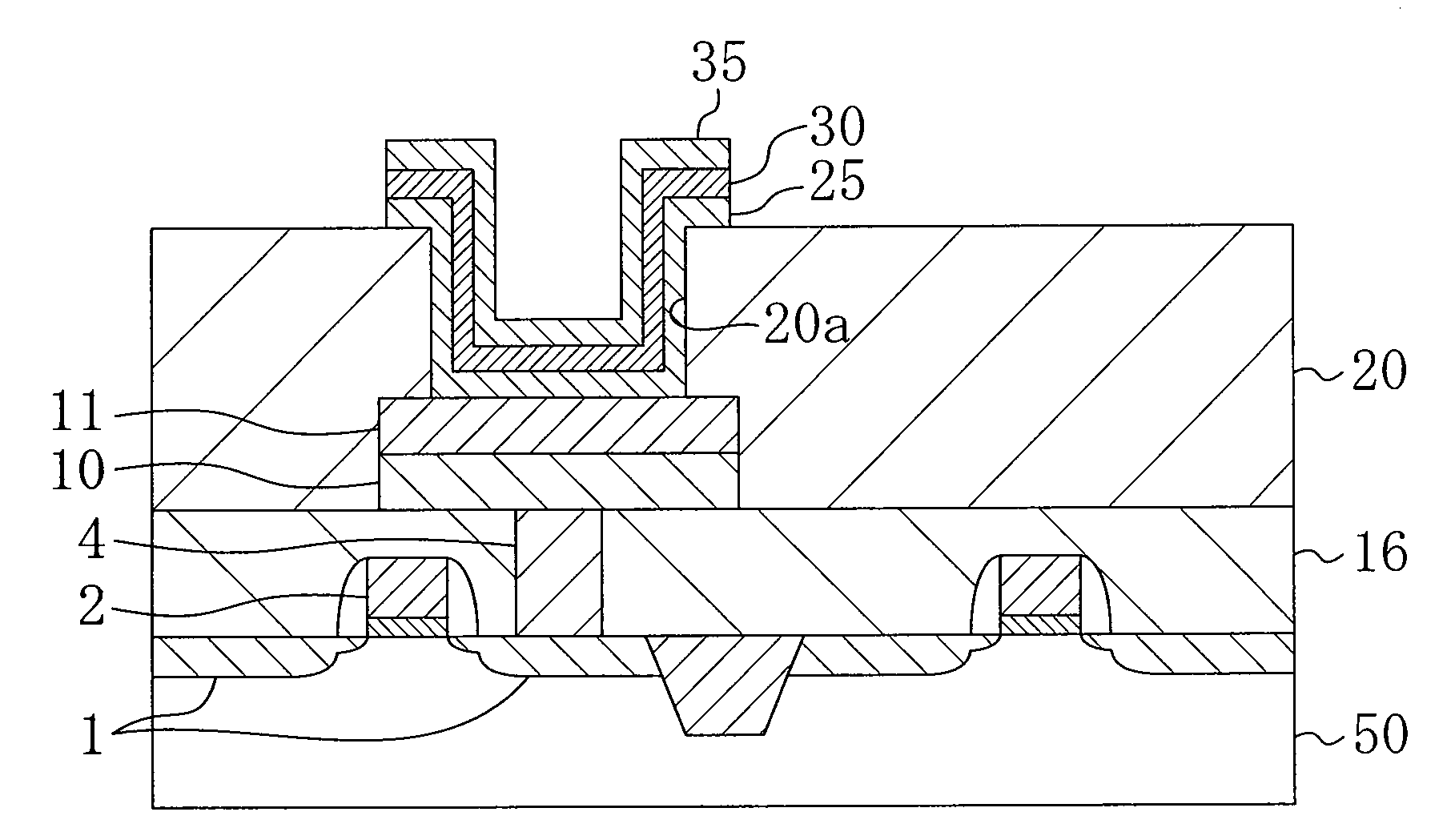
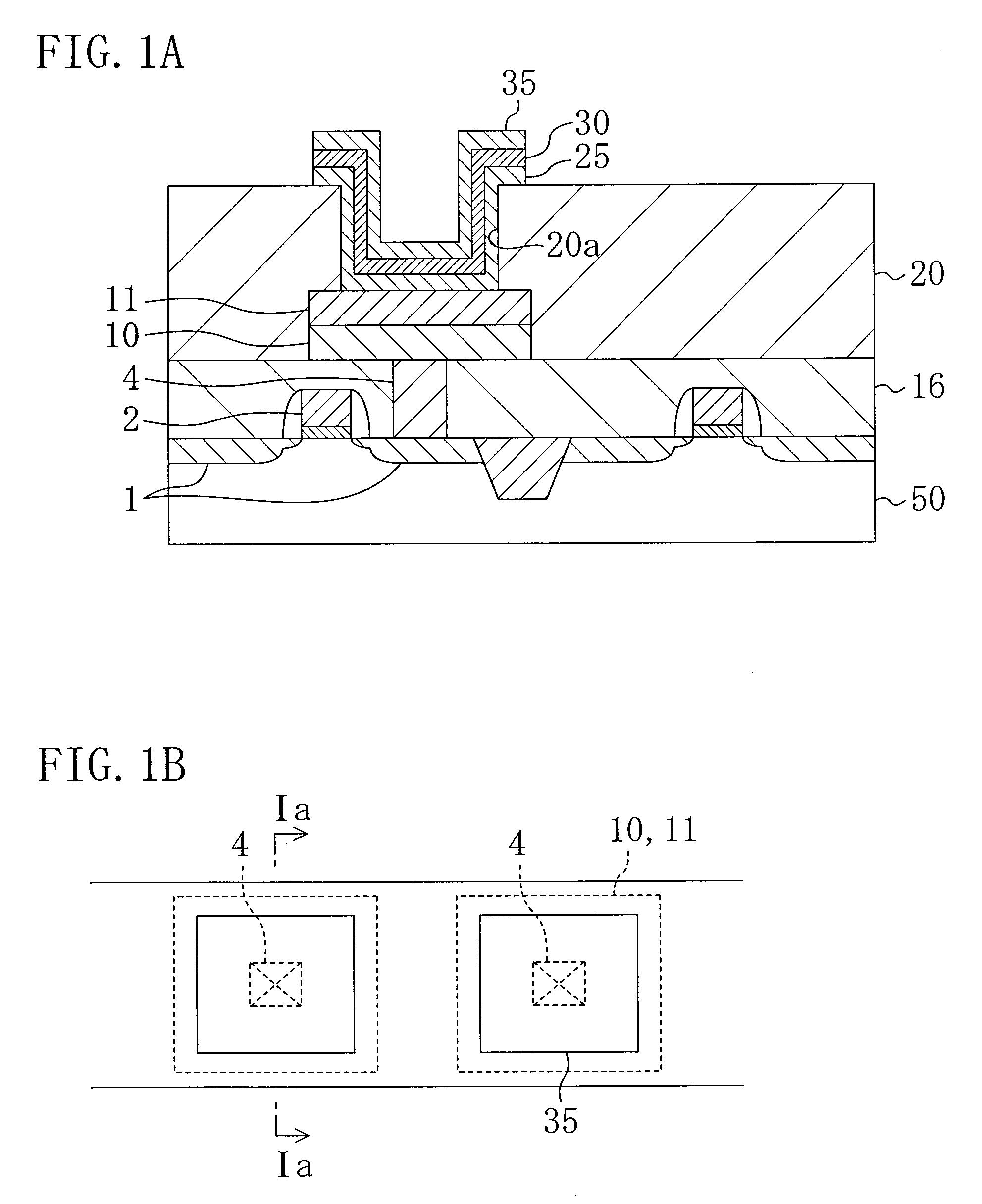
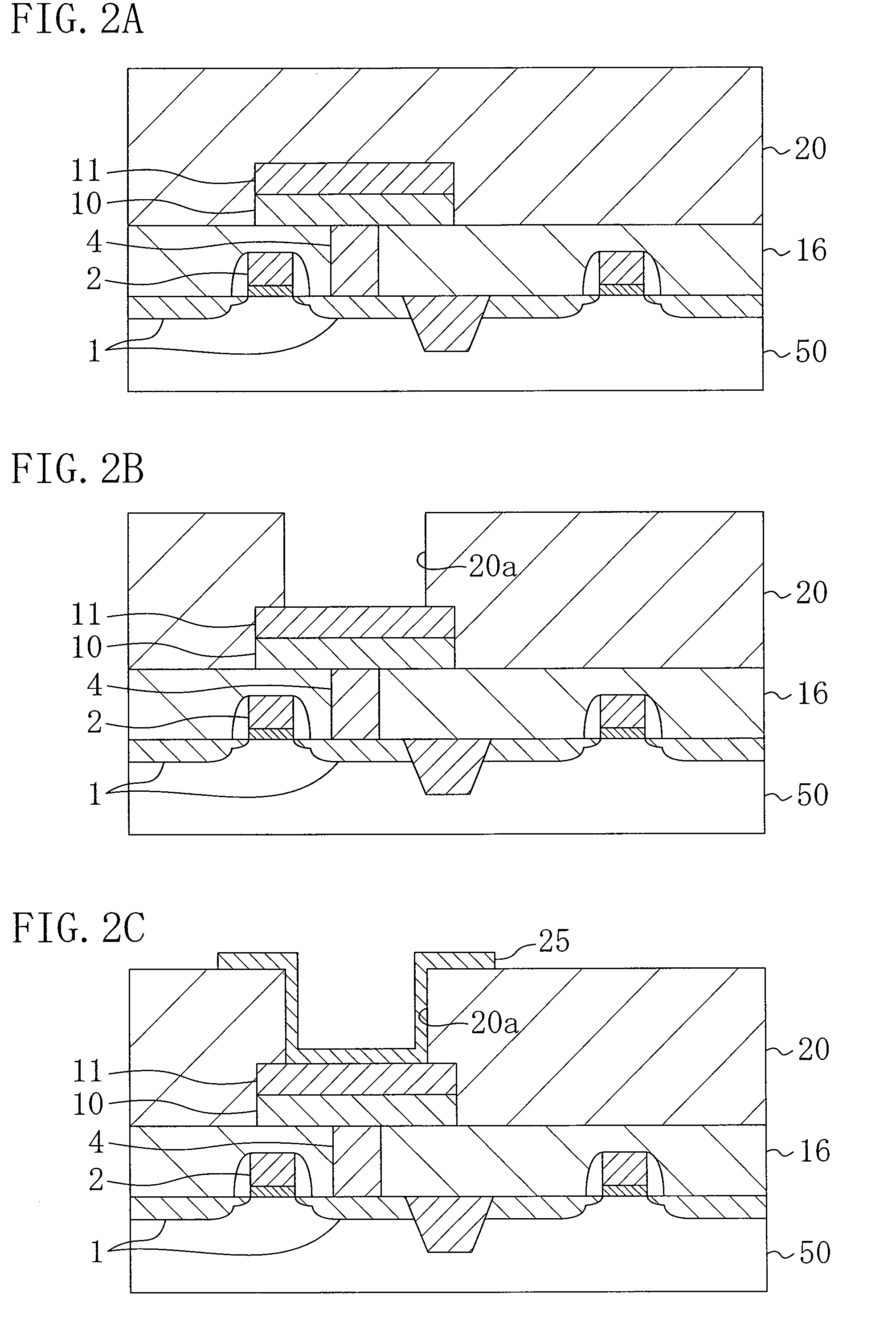
[0071]FIGS. 1A and 1B show the main part of a semiconductor storage device in accordance with Example Embodiment 1, in which FIG. 1A is a cross-sectional view taken along the line Ia-Ia in FIG. 1B, and FIG. 1B is a plan view.

[0072]As shown in FIG. 1A, in the semiconductor storage device in accordance with the present exemplary embodiment, transistors including source / drain regions 1 and a gate electrode 2 are integrated in a semiconductor substrate 50, and a first interlayer insulating film 16 made of silicon oxide (SiO2), for example, is formed on the semiconductor substrate 50 to entirely cover the transistors. A contact plug 4 made of tungsten or polysilicon and connected to a source / drain region 1 of a transistor is formed in the interlayer insulating film 16. On the interlayer insulating film 16, an oxygen barrier film 10 is formed to be connected to the contact plug 4. The oxygen barrier film 10 ...

example embodiment 2

[0089]Example Embodiment 2 will be described below with reference to FIG. 5 to FIG. 7.

[0090]FIGS. 5A and 5B show the main part of a semiconductor storage device in accordance with Example Embodiment 2, in which FIG. 5A is a cross-sectional view taken along the line Va-Va in FIG. 5B, and FIG. 5B is a plan view. In FIG. 5, the same reference numerals are assigned to the same elements as those in FIG. 1 for omitting the description thereof.

[0091]Difference of the semiconductor storage device of Example Embodiment 2 from that of Example Embodiment 1 lies in that, as shown in FIG. 5A, a hole opening 20a formed in the second interlayer insulating film 20 passes through a conductive adhesive layer 11a and exposes the oxygen barrier film 10 therebelow. The hole opening 20a passing through the conductive adhesive layer 11a allows the conductive adhesive layer 11a to be in contact with the bottom electrode 25 at the wall surface of the hole opening 20a which includes the bottom corner thereof...

example embodiment 3

[0102]Example Embodiment 3 will be described below with reference to FIG. 8 to FIG. 11.

[0103]FIG. 8 shows the section of the main part of a semiconductor storage device in accordance with Example Embodiment 2. In FIG. 8, the same reference numerals are assigned to the same elements as those in FIG. 1 for omitting the description thereof.

[0104]Difference of the semiconductor storage device of Example Embodiment 3 from that of Example Embodiment 2 lies in that, as shown in FIG. 8, a conductive adhesive layer is formed with a stacked film of a first conductive adhesive layer 11b and a second conductive adhesive layer 13 thereon, and the second conductive adhesive layer 13 is opened at its central part to expose the first conductive adhesive layer 11b. Accordingly, the bottom electrode 25 is in contact with the first conductive adhesive layer 11b at the bottom corner of the hole opening 14a, while being in contact with the second conductive adhesive layer 13 at the lower part of the wal...


PUM


Abstract

A semiconductor storage device includes: a first conductive adhesive layer selectively formed over a semiconductor substrate; an insulating film formed on the semiconductor substrate to cover the first conductive adhesive layer and having an opening exposing a central part of the first conductive adhesive layer; and a capacitive element including a bottom electrode formed along a bottom surface and a wall surface of the opening, a capacitive insulating film formed on the bottom electrode, and a top electrode formed on the capacitive insulating film. The first conductive adhesive layer is in contact with the bottom electrode only at a bottom surface part of the opening which includes a corner where the bottom surface of the opening meets the wall surface thereof.

Description

CROSS REFERENCE TO RELATED APPLICATIONS[0001]This non-provisional application claims priority under 35 U.S.C. §119(a) on Patent Application No. 2008-099420 filed in Japan on Apr. 7, 2008, the entire contents of which are hereby incorporated by reference.TECHNICAL FIELD[0002]The present disclosure relates to semiconductor storage devices and manufacturing methods thereof, and particularly relates to a semiconductor storage device, which is a ferroelectric memory device or a high dielectric constant memory device using a dielectric material, and a manufacturing method thereof.BACKGROUND ART[0003]In development of ferroelectric memory devices, mass production of memory devices having small capacities of 1 kbit to 64 kbit and employing a planar structure have started first, and recently, memory devices in a stack structure having large capacities of 256 kbit to 4 Mbit are now developed dominantly. In the ferroelectric memory devices in a stack structure, contact plugs electrically conne...

Claims


Application Information

Patent Timeline
Patent Type & Authority Applications(United States)
IPC IPC(8): H01L29/92H01L21/02
CPCH01L27/11507H01L28/75H01L28/55H10B53/30
Inventor KUTSUNAI, TOSHIE
Owner PANASONIC CORP
Why Eureka
Try Eureka