Shift register circuit, display panel, and electronic apparatus

a register circuit and display panel technology, applied in the direction of digital storage, instruments, semiconductor devices, etc., to achieve the effects of enhancing the stability of operation, reducing power consumption, and preventing leakag

Inactive Publication Date: 2009-10-08
SONY CORP
View PDF3 Cites 54 Cited by
  • Summary
  • Abstract
  • Description
  • Claims
  • Application Information

AI Technical Summary

Benefits of technology

[0078]Specifically, the output pulse is used to charge the interconnect capacitors of the nodes A and B. Therefore, the clock signal CK is desired to have such drive ability as to drive this high load capacitance. Specifically, it is desired to increase the size of the buffer circuit that supplies the clock signal.
[0146]The above-described shift register circuits based on thin film transistors with channels of the same conductivity type are less susceptible to the influence of characteristic variation due to manufacturing variation and allow higher-speed operation and lower power consumption compared with the related-art circuit.

Problems solved by technology

However, in mounting thereof, the influence of off-leakage and coupling needs to be taken into consideration.

Method used


Image

  • Shift register circuit, display panel, and electronic apparatus
  • Shift register circuit, display panel, and electronic apparatus
  • Shift register circuit, display panel, and electronic apparatus

Examples


Embodiment Construction

[0226]The following description will deal with an example in which an embodiment of the present invention proposed by this specification is applied to a drive circuit in an active-matrix driven display panel.

[0227]Well-known or publicly-known techniques in the related-art technical field are applied to part that is not particularly illustrated or described in the present specification.

[0228]It should be noted that the form examples to be described below is merely one embodiment example of the present invention and the present invention is not limited thereto.

(A) SYSTEM CONFIGURATION OF DISPLAY PANEL

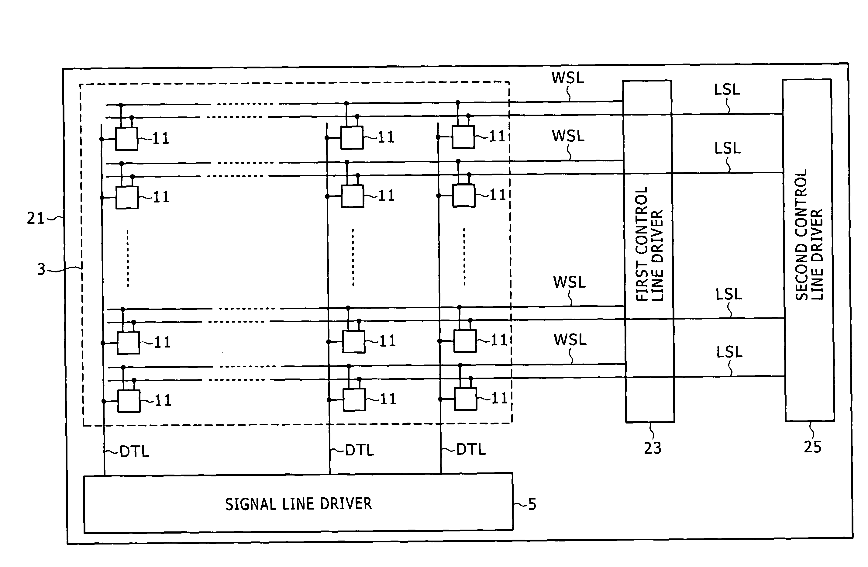
[0229]The following form example relates to an organic EL panel. FIG. 20 shows a system configuration example of an organic EL panel according to the form example. The same parts in FIG. 20 as those in FIG. 1 are given the same numerals and symbols.

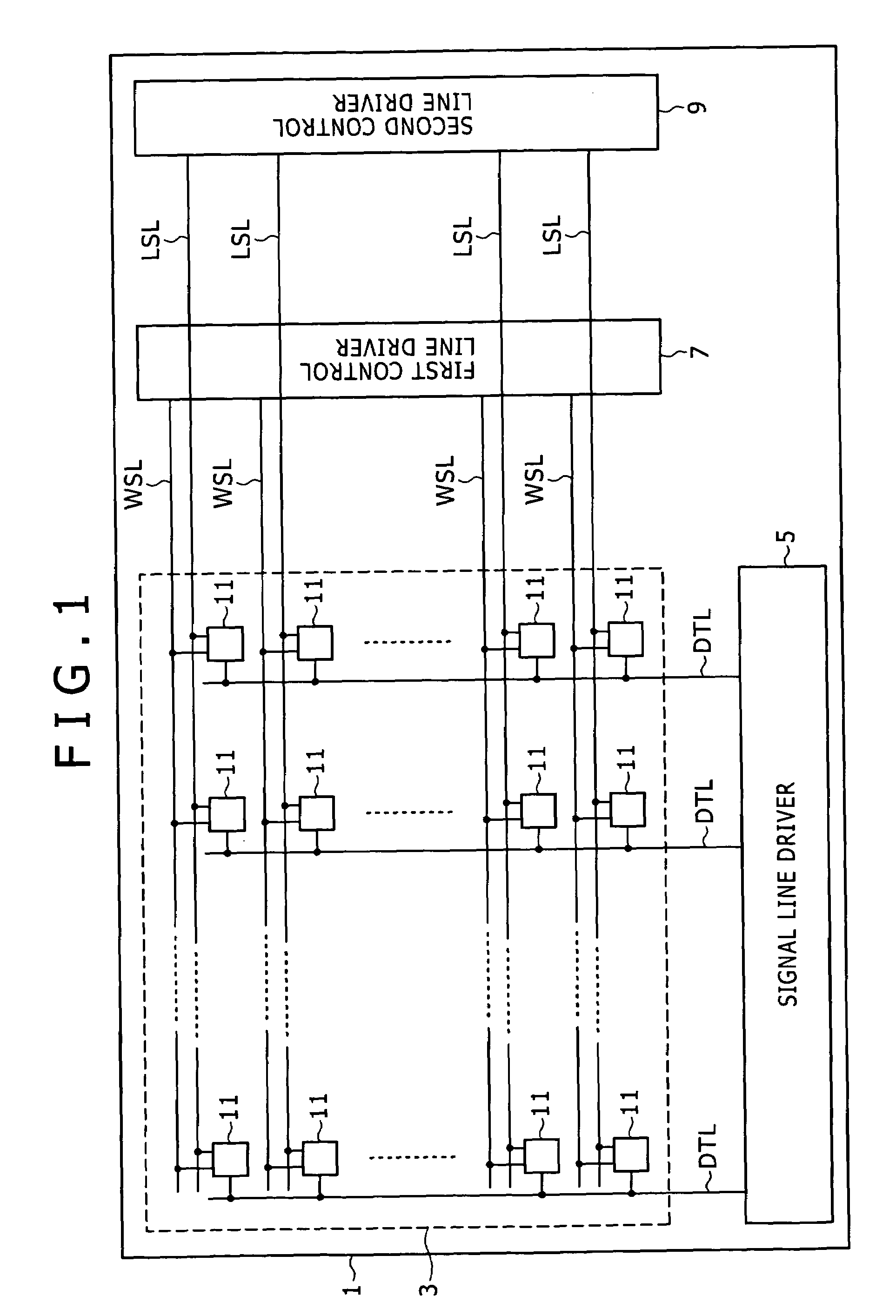
[0230]An organic EL panel 21 according to the form example includes a pixel array part 3, a signal line driver 5, a first control line driver...


PUM


Abstract

Disclosed herein is a shift register circuit that is formed on an insulating substrate with thin film transistors having channels of the same conductivity type and includes shift stages, each of the shift stages including: a first thin film transistor; a second thin film transistor; a 3(1)-th thin film transistor; a 3(2)-th thin film transistor; a 4(1)-th thin film transistor; a 4(2)-th thin film transistor; a fifth thin film transistor; and a sixth thin film transistor.

Description

BACKGROUND OF THE INVENTION[0001]1. Field of the Invention[0002]The invention to be described in this specification relates to a shift register circuit formed on an insulating substrate with thin film transistors including channels of the same conductivity type. The invention to be described in this specification has modes as a shift register circuit, a display panel, and electronic apparatus.[0003]2. Description of the Related Art[0004]A low-temperature poly-silicon (LTPS) process allows circuit formation with both an NMOS thin film transistor (TFT) and a PMOS thin film transistor. Therefore, it is general to manufacture a circuit (so-called CMOS circuit) with these two kinds of thin film transistors in the low-temperature poly-silicon process.[0005]However, the manufacturing of the CMOS circuit inevitably involves increase in the number of steps because two kinds of thin film transistors are used. This increase in the number of steps causes the lowering of the productivity and inc...

Claims


Application Information

Patent Timeline
Patent Type & Authority Applications(United States)
IPC IPC(8): G09G5/00G11C19/28
CPCG09G3/3233G09G3/3266G09G2300/0819G09G2300/0842H01L29/41733G09G2310/0286G09G2320/043G11C19/184G11C19/28G09G2300/0866H10K59/12G09G3/3241G09G2300/0857G09G2320/0613G09G2300/04
Inventor JINTA, SEIICHIRO
Owner SONY CORP
Why Eureka
Try Eureka