

Deposition method for high-k dielectric materials
a dielectric material and liquid phase technology, applied in the direction of liquid/solution decomposition chemical coating, solid/suspension decomposition chemical coating, coating, etc., can solve the problems of film quality, film continuity, film contamination, etc., and achieve the effect of improving the film quality and film quality
- Summary
- Abstract
- Description
- Claims
- Application Information
AI Technical Summary
Problems solved by technology
Method used
Image

Examples
Embodiment Construction
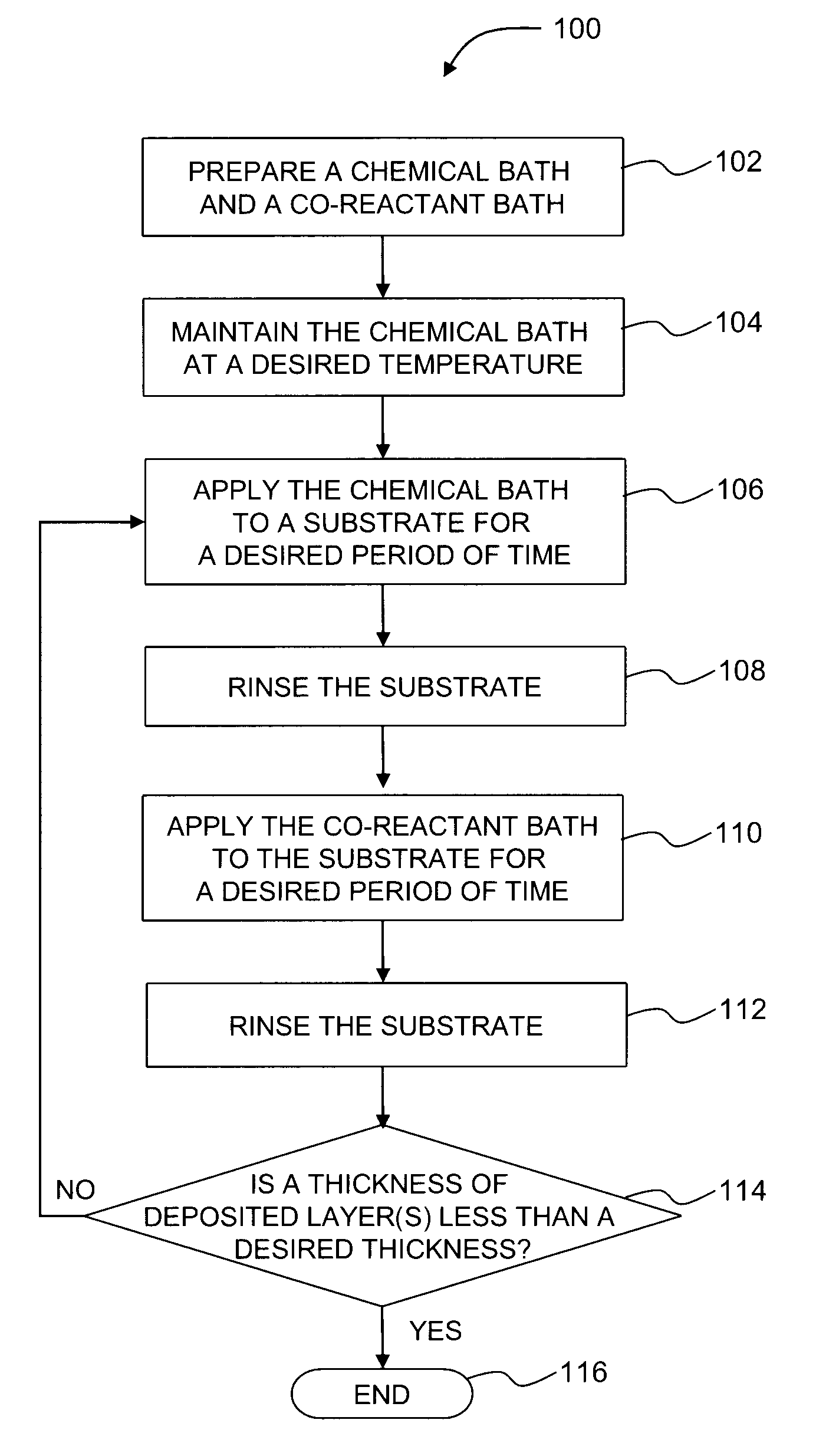
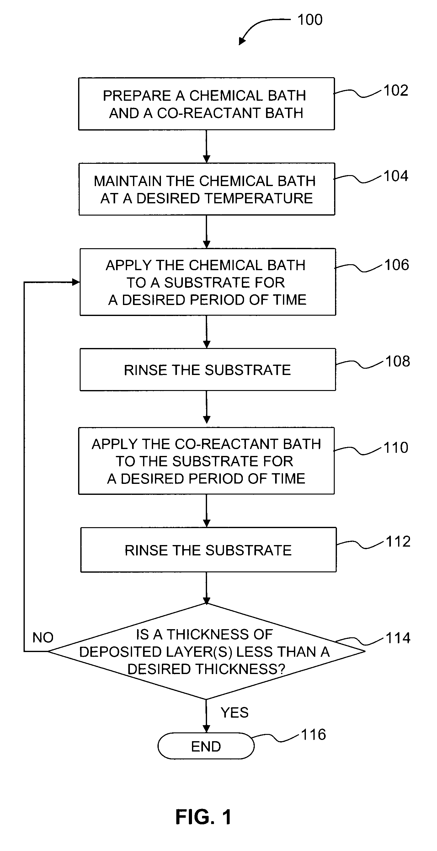
[0008]In the following description, numerous specific details are set forth in order to provide a thorough understanding of various illustrative embodiments of the present invention. It will be understood, however, to one skilled in the art, that embodiments of the present invention may be practiced without some or all of these specific details. In other instances, well known process operations have not been described in detail in order not to unnecessarily obscure pertinent aspects of embodiments being described. In the drawings, like reference numerals refer to same or similar functionalities or features throughout the several views.
[0009]Embodiments of the invention relate to liquid phase deposition of a metal oxide to provide a high-k dielectric layer on a semiconductor substrate. The deposition method involves applying chemical and co-reactant baths separated by rinsing baths to deposit stacked layers of a metal oxide until a desired thickness is obtained. The chemical bath inc...
PUM
| Property | Measurement | Unit |
|---|---|---|
| Temperature | aaaaa | aaaaa |
| Temperature | aaaaa | aaaaa |
| Time | aaaaa | aaaaa |
Abstract
Description
Claims
Application Information