Thermal control of deposition in dip pen nanolithography

a technology of nanolithography and thermal control, which is applied in the field of thermal control of deposition in dippen nanolithography, can solve the problems of loss of registry between the tip and the surface, the inability of the coated tip to be used for imaging purposes, and the further limitation of dpn

Inactive Publication Date: 2009-10-15
THE UNITED STATES OF AMERICA AS REPRESENTED BY THE SECRETARY OF THE NAVY
View PDF33 Cites 3 Cited by
  • Summary
  • Abstract
  • Description
  • Claims
  • Application Information

AI Technical Summary

Problems solved by technology

With this technology, however come some limitations.
Unfortunately, this can often lead to a loss of registry between the tip and the surface.
Another drawback to DPN is that a coated tip cannot be used for imaging purposes while in contact mode without causing contamination—deposition of unwanted ink.
DPN is further limited in that besides changing the ink, the tip, or the tip's speed, there is little control over the deposition rate once a molecule has been coated onto the tip.
This ambient temperature mobility requirement limits the types of inks that may be used in DPN and results in “bleeding” or spreading out of the ink once it is deposited onto a surface, which in turn limits the precision of structures that can be created with DPN.
Because of this necessary volatility of the inks used in DPN, the process cannot be performed in a vacuum; the ink would evaporate too quickly and contaminate the system.
However, each one of these references suffers from one or more of the following disadvantages: inability to image in contact mode without contaminating, inability to turn deposition on or off, and inability to control excess diffusion of ink once deposited.

Method used


Image

  • Thermal control of deposition in dip pen nanolithography
  • Thermal control of deposition in dip pen nanolithography
  • Thermal control of deposition in dip pen nanolithography

Examples


example 1

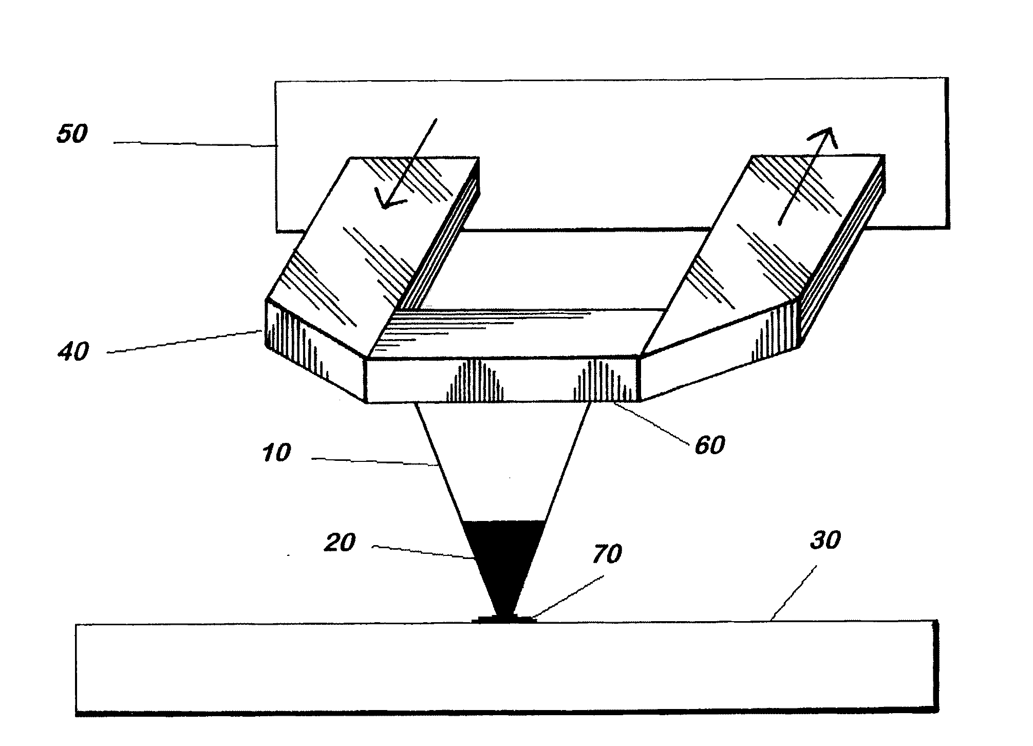
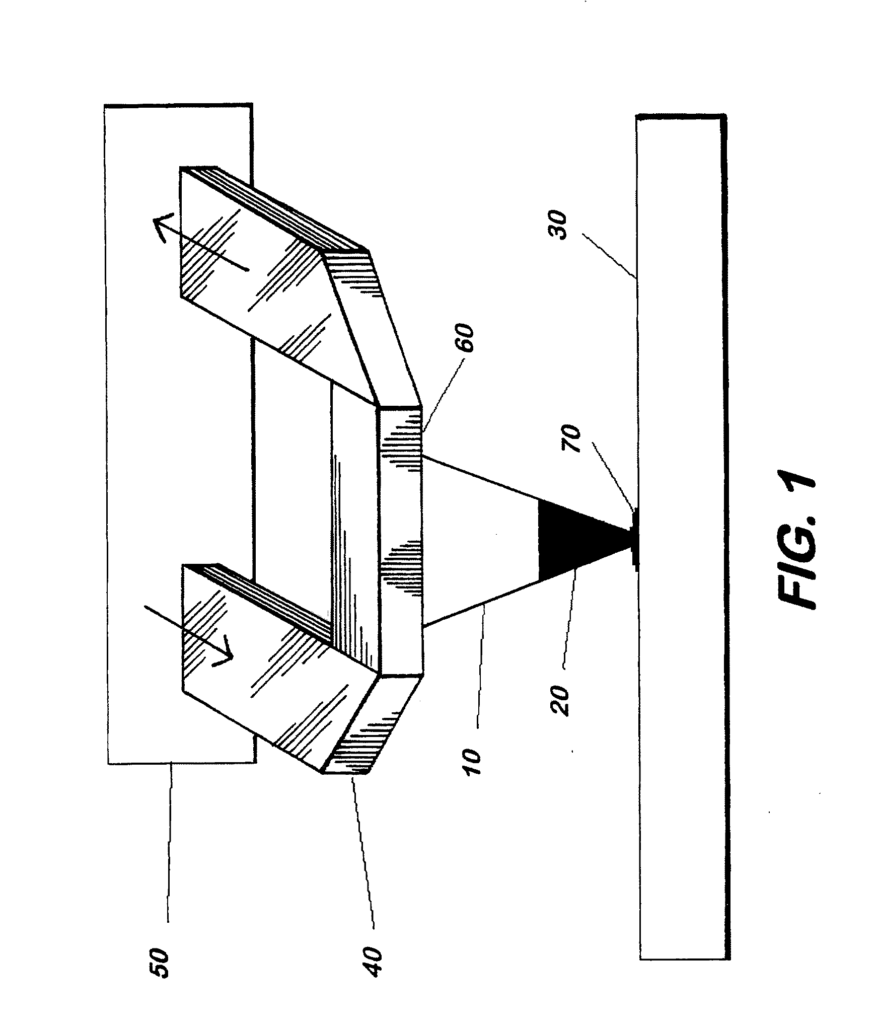
[0039]Deposition of OPA—An AFM tip, coated with OPA in the manner described above, was rastered over four, 500 nanometer square regions on a mica substrate at 2 Hz and 128 lines per scan, or for a total scan time of 256 s. For each square, the temperature of the cantilever was increased, finally exceeding OPA's melting temperature. When the temperature of the tip was held below OPA's Tm, either at 25° C. or at 57° C., no patterned squares were observed. Raising the tip temperature to 98° C., near OPA's Tm, resulted in light deposition. The average height of this area was 1.1 nm, which is slightly less than one-half the height of a full monolayer. Robust deposition was finally seen when the cantilever temperature was raised to 122° C., creating a square pattern with a height of 2.5 nm, indicative of a full monolayer, as shown in FIG. 3. The corresponding friction image, shown in FIG. 4, confirms OPA deposition. The binding of OPA to mica exposes a methyl terminal group, which would r...

example 2

[0042]Deposition of PDDT—tDPN was used to deposit conducting polymer between electrodes. The polymer was poly(3-dodecylthiophene) (PDDT), a semiconducting polymer useful for organic FETs. The tip was heated to ˜200° C. under nitrogen (to avoid oxidation). The tip was then scanned from one electrode to the other for 2 minutes. The deposited line was 20 nm thick and 150 nm wide and spaned an 800 nm wide gap.

example 3

[0043]Deposition of Indium—For the repair of nanoscale circuits or of the photomasks used to make modem circuitry, it is important to be able to write small, conducting wires. tDPN was used to pattern indium, a low melting point metal and a common solder. FIG. 7 shows a series of 3 μm lines written at a tip speed of 3 μm / s. Each line was traversed 64 times (i.e., 32 trace / retraces) by the depositing tip. The top two lines written at 95° C. and 135° C. do not show, the faint line at bottom left was written at 156° C. which is close to the melting temperature of the indium, 156.6° C. The line at bottom right was written at 196° C., which is well above the melting temperature of indium, and demonstrates robust deposition at this temperature.


PUM

PropertyMeasurementUnit
melting temperaturesaaaaaaaaaa
room temperatureaaaaaaaaaa
timeaaaaaaaaaa

Abstract

The present invention describes an apparatus for nanolithography and a process for thermally controlling the deposition of a solid organic “ink” from the tip of an atomic force microscope to a substrate. The invention may be used to turn deposition of the ink to the substrate on or off by either raising its temperature above or lowing its temperature below the ink's melting temperature. This process may be useful as it allows ink deposition to be turned on and off and the deposition rate to change without the tip breaking contact with the substrate. The same tip can then be used for imaging purposes without fear of contamination. This invention can allow ink to be deposited in a vacuum enclosure, and can also allow for greater spatial resolution as the inks used have lower surface mobilities once cooled than those used in other nanolithography methods.

Description

[0001]This application is a divisional application of U.S. Pat. No. 7,541,026, which claims the benefit of U.S. Provisional Application No. 60 / 603,508, filed on Aug. 18, 2004.BACKGROUND OF THE INVENTION[0002]1. Field of the Invention[0003]This invention relates to an apparatus and method for thermally controlling deposition in Dip-Pen Nanolithography, or DPN (Dip-Pen Nanolithography, and DPN are registered trademarks of Nanoink).[0004]2. Description of the Prior Art[0005]The ability to create ever smaller structures and patterns is the key to producing smaller and faster electronics. Some of the newest technologies allow the creation of structures on the nanometer, or 10−9 meter, scale. One of these technologies is DPN, which is described in U.S. Pat. No. 6,635,311 and is incorporated herein by reference (all patent and publication references included in this specification hereinafter are also incorporated by reference). DPN is a method for depositing molecules onto a surface with t...

Claims


Application Information

Patent Timeline
Patent Type & Authority Applications(United States)
IPC IPC(8): B05C11/00G01Q10/00G01Q60/24G01Q80/00
CPCB82Y10/00B82Y40/00G01Q80/00Y10S977/855Y10S977/851Y10S977/849Y10S977/857G03F7/0002G03F7/70891H01L21/67248
Inventor SHEEHAN, PAUL E.WHITMAN, LLOYD J.KING, WILLIAM P.
Owner THE UNITED STATES OF AMERICA AS REPRESENTED BY THE SECRETARY OF THE NAVY
Why Eureka
Try Eureka