Electrochemical miniaturization of organic micro-and nanostructures

a micro- and nano-structure technology, applied in the field of electrochemical miniaturization of organic micro- and nano-structures, can solve the problem that the dpn cannot rival the available printing process, and achieve the effect of reducing the size of the dpn

Inactive Publication Date: 2009-11-03
NORTHWESTERN UNIV
View PDF2 Cites 0 Cited by
  • Summary
  • Abstract
  • Description
  • Claims
  • Application Information

AI Technical Summary

Benefits of technology

[0009]Another embodiment of the present invention provides a method of miniaturizing the size of a first organic structure in the presence of a second organic structure on a substrate by applying an electrical potential to the substrate such that the first organic structure is electrochemically desorbed from the outside of the organic structure without negatively affecting the second organic structure. In this embodiment, the first organic structure may make contact with the substrate through a selenium atom and the second organic molecule may make contact with the substrate through a sulfur atom Additionally, in this embodiment, the first organic structure may contain a hexadecanoic acid tail group and the second organic molecule may contain an octadecane tail group.
[0010]Another embodiment of the present invention provides a method of miniaturizing the size of organic structures on a substrate by applying a first electrical potential to the substrate such that the first organic structure is electrochemically desorbed from the outside of the organic structure without negatively affecting the second organic structure and then applying a second electrical potential to the substrate such that the second organic structure is electrochemically desorbed from the outside of the organic structure without negatively affecting the first organic structure. The electrical potentials applied in this embodiment may be applied in the same or different electrolyte solutions. The method of this embodiment may also be used to form an organic structure on a conductive substrate by forming a first organic structure on a conductive substrate and forming at least one additional organic structure on the same conductive substrate. The first organic structure is then selectively removed or miniaturized leaving the additional organic structures on the substrate. This method may then be extended to incorporate another chemical onto the substrate in place of the first desorbed organic structure amongst the remaining additional organic structures.

Problems solved by technology

Although advances have recently extended single-pen DPN approaches to parallel multi-pen approaches, the throughput of DPN cannot rival the available printing processes.

Method used


Image

  • Electrochemical miniaturization of organic micro-and nanostructures
  • Electrochemical miniaturization of organic micro-and nanostructures
  • Electrochemical miniaturization of organic micro-and nanostructures

Examples


example 1

[0047]This example provides details of substrate preparation, DPN or microcontact printing of organic structures, and electrochemical whittling procedures. A polycrystalline Au film substrate was prepared by evaporating 10 nm of Ti (99.99%; Alfa Aesar, Ward Hill, Mass.) on SiOx followed by 60 nm of Au (99.99%; Alfa Aesar, Ward Hill, Mass.) in an evaporator chamber (Edwards Auto 306) at room temperature (Weinberger et al., Adv. Mater. 12:1600 (2000)). Au ball substrates were prepared from approximately 0.5 cm lengths of Au wire (99.99%, 0.5 mm in diameter; Alfa Aesar, Ward Hill, Mass.) by using a hydrogen / oxygen flame (Ross et al., Langmuir 9:632 (1993)).

[0048]DPN of organic nanostructures was performed using an atomic force microscope (AFM, CP, Veeco, Santa Barbara, Calif.) equipped with a 100 μm scanner with closed-loop scan control and commercial lithography software (DPNWrite™, DPN System-1, NanoInk Inc., Chicago, Ill.). Gold-coated Si3N4 AFM cantilevers (Microlever, Veeco, Santa...

example 2

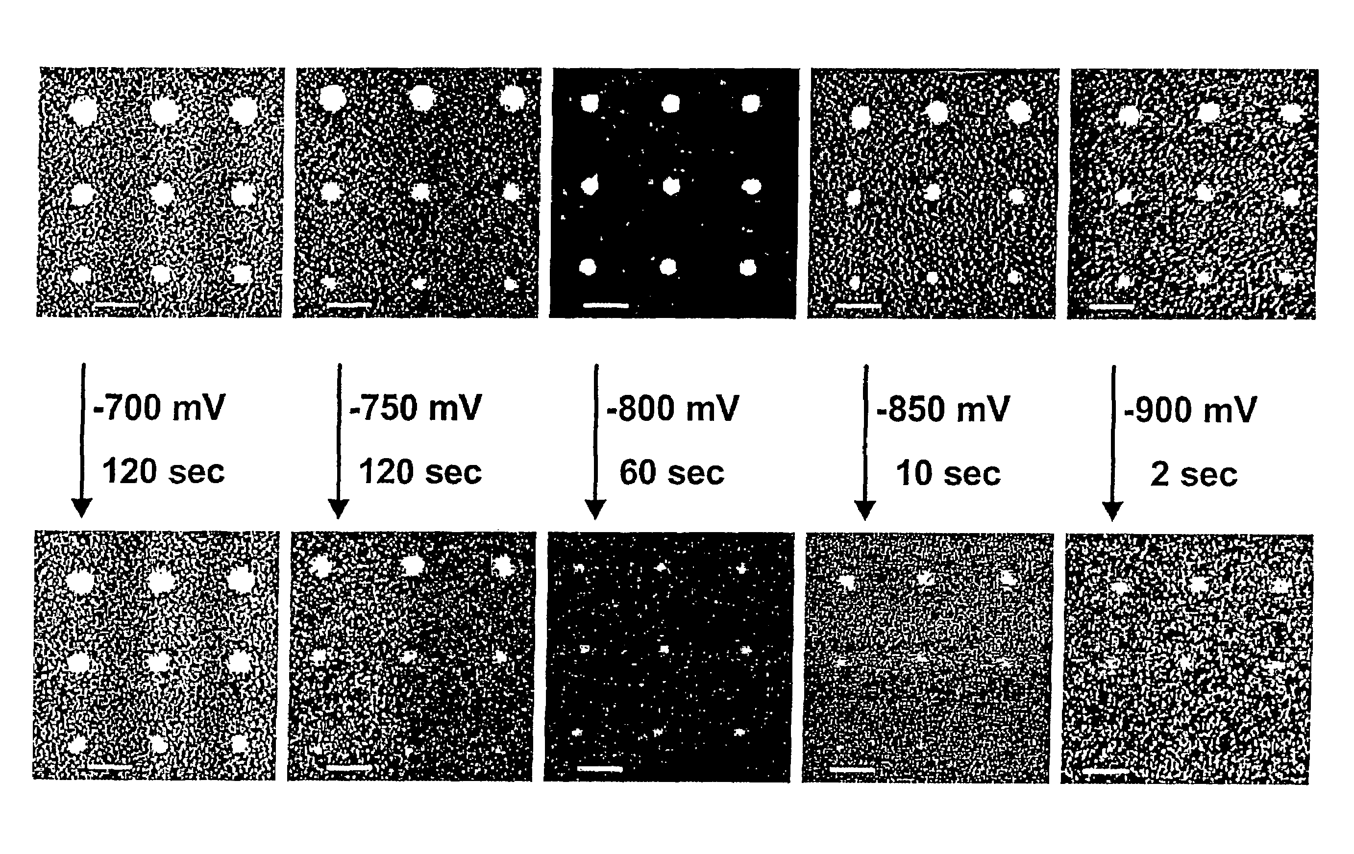
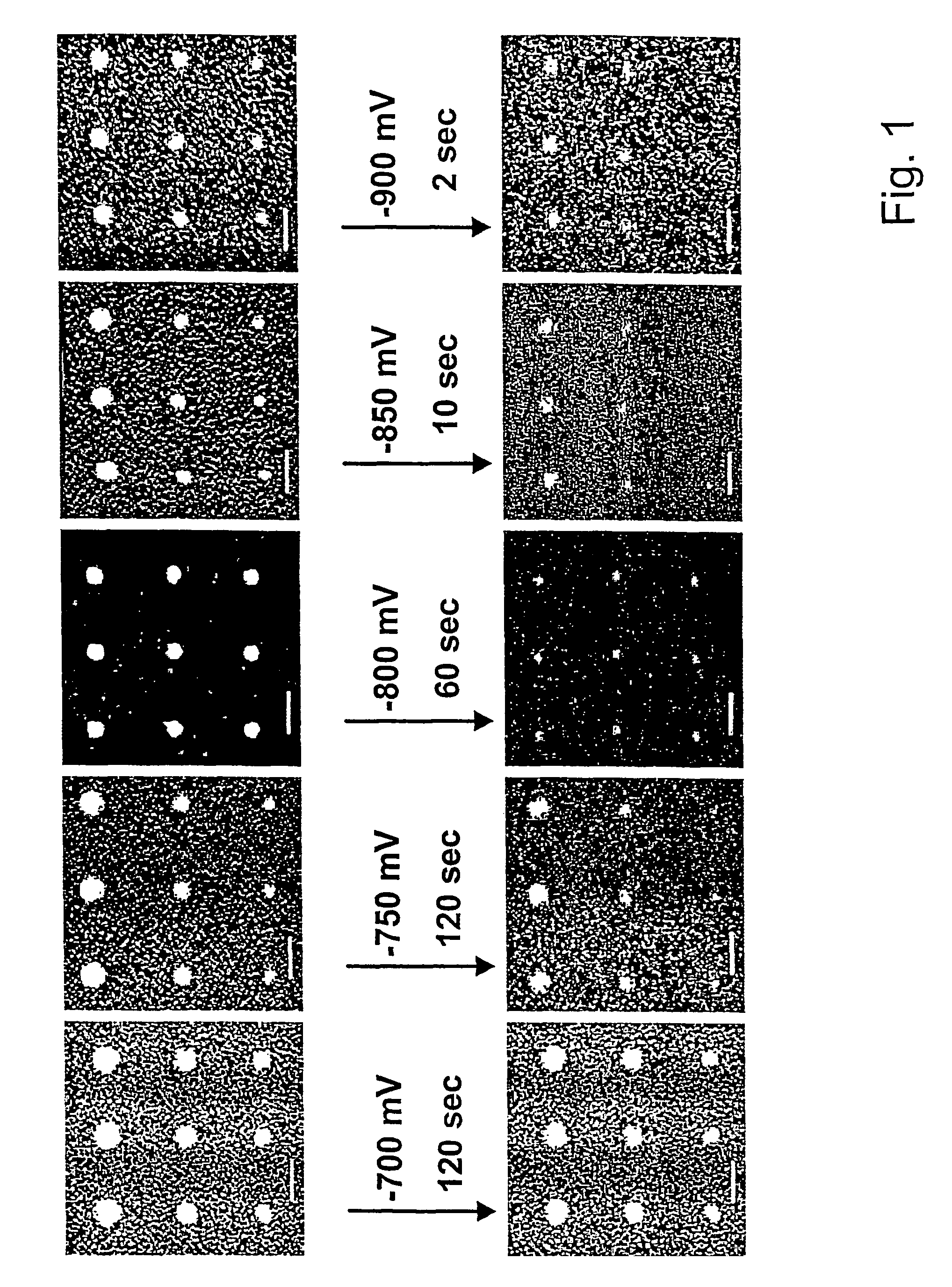
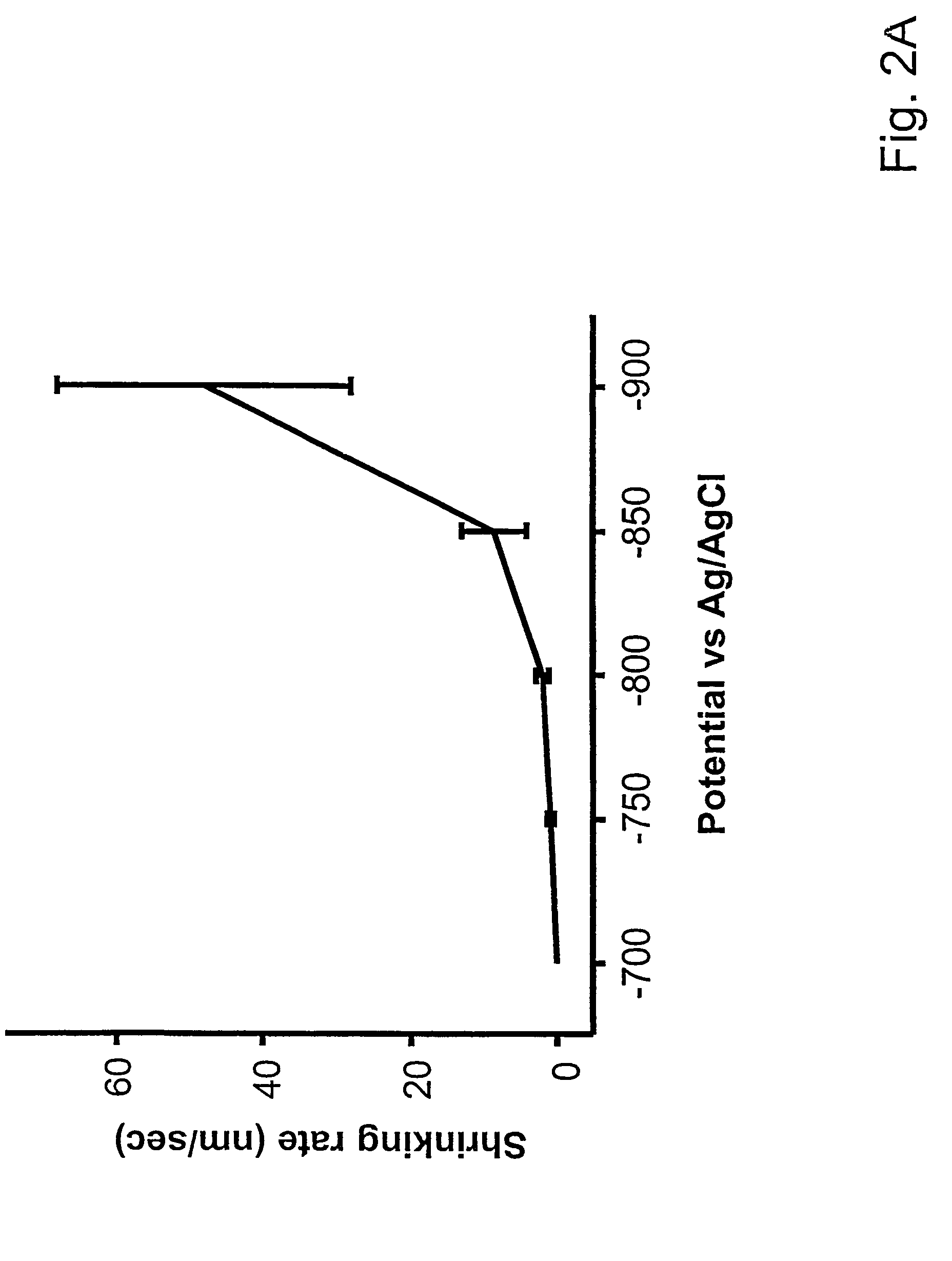
[0052]This example demonstrates the technique of electrochemical desorption on organic nanostructures using different electrochemical potentials. FIG. 1 shows the electrochemical desorption of MHA nanostructures at different potentials. A threshold voltage of about −750 mV vs Ag / AgCl was found, above which no desorption could be detected under our experimental conditions. As seen in FIG. 1, when the substrate was held at a potential of −700 mV in an aqueous solution of 0.5 M MOH (where M=K, Na or Li) for two minutes, the MHA dot size (approximately 300 nm) showed no detectable change. These results indicate that when a potential of −750 mV is applied to a substrate, the MHA dots begin to shrink at a rate of approximately 50 nm / min, see FIG. 1. Generally, more negative potentials accelerate feature size reduction. Under a potential of −800 mV, the desorption rate becomes approximately 120 nm / min. As the potential becomes more negative, the MHA dots shrink so fast that the desorption ...

example 3

[0053]This example demonstrates the effect of electrochemical desorption on nanostructures in a variety of electrolytes. As shown in FIG. 3, when a potential of −750 mV vs Ag / AgCl is applied to the substrate, the MHA dots start to shrink in both NaOH and LiOH solutions. Again, no obvious size change was detected when the substrate potential was held at −700 mV or more positive for several minutes in both NaOH (compare FIGS. 4A and 4B) and LiOH (compare FIGS. 4C and 4D) solutions.

[0054]However, as shown in Table 1, the desorption rates of the MHA nanostructures in LiOH, NaOH, and KOH solutions were markedly different. At an electrode potential of −750 mV, the average desorption rate in 0.5 M aqueous NaOH solution was 16±7 nm / min, while in 0.5 M aqueous LiOH solution the desorption rate was 6±3 nm / min. The desorption rates in both NaOH and LiOH solutions are much lower than that in KOH solution. Although the desorption rate in LiOH solution was much slower, there was still a strong de...


PUM

PropertyMeasurementUnit
electrical potentialaaaaaaaaaa
feature sizeaaaaaaaaaa

Abstract

The invention provides a simple and convenient strategy for reducing the dimensions of organic micro- and nanostructures on metal surfaces. By varying electrochemical desorption conditions, organic structures patterned by Dip-Pen Nanolithography or any of the micro-contact printing procedures can be gradually desorbed in a controlled fashion. The electrochemical desorption is initiated at the exterior of the feature and moves inward as a function of time. The desorption process and adsorbate desorption are modified and controlled as a function of substrate morphology, adsorbate head and tail groups, and electrolyte solvent and salt. Different nanostructures made of different adsorbates can be miniaturized based upon judicious selection of adsorbate and supporting electrolyte.

Description

CROSS REFERENCE TO RELATED APPLICATIONS[0001]This application is the National Stage of International Application No. PCT / US03 / 2 1220 filed Jul. 7, 2003 which claims priority to U.S. Provisional Patent Application Serial No. 60 / 394,141, filed Jul. 5, 2002, entitled “Electrochemical Whittling of Organic Nanostructures,” the disclosure of which is incorporated herein its entirety by this reference.STATEMENT REGARDING FEDERALLY SPONSORED RESEARCH[0002]This invention was made with Government support under Grant No. DAAD19-00-1-0414 awarded by DARPA, Grant No. DUIRINT F49620-01-l-0401 awarded by AFOSR and Grant No. NSEC EEC-0118025 awarded by the NSF. The Government has certain rights in this invention.FIELD OF THE INVENTION[0003]The invention lies in the field of forming and varying the size of organic microstructures and nanostructures.BACKGROUND OF THE INVENTION[0004]There are a variety of methods for printing and constructing organic structures on surfaces, and these methods are leadi...

Claims


Application Information

Patent Timeline
Patent Type & Authority Patents(United States)
IPC IPC(8): C25F3/00C23C22/82C25F1/00B01L3/00C40B60/14
CPCH01L51/0017B81C1/00111B81C1/00714B82Y10/00B82Y30/00B82Y40/00C25F1/00C40B40/04C40B60/14G03F7/0002B01J2219/00387B01J2219/00605B01J2219/00612B01J2219/0063B01J2219/00637B01L3/5027H01L51/0006B01J2219/00436H10K71/125H10K71/231
Inventor MIRKIN, CHAD A.ZHANG, YISALAITA, KHALID
Owner NORTHWESTERN UNIV
Why Eureka
Try Eureka