
Preparation method of patterned titanium dioxide micro structure
A technology of titanium dioxide and microstructure, applied in the direction of titanium dioxide, replication/marking methods, titanium oxide/hydroxide, etc., can solve the problems of low selectivity of self-assembled membranes, reduce experimental costs, etc., and achieve improved clarity and boundary resolution High efficiency, easy mass production, simple operation
- Summary
- Abstract
- Description
- Claims
- Application Information
AI Technical Summary
Problems solved by technology
Method used
Image

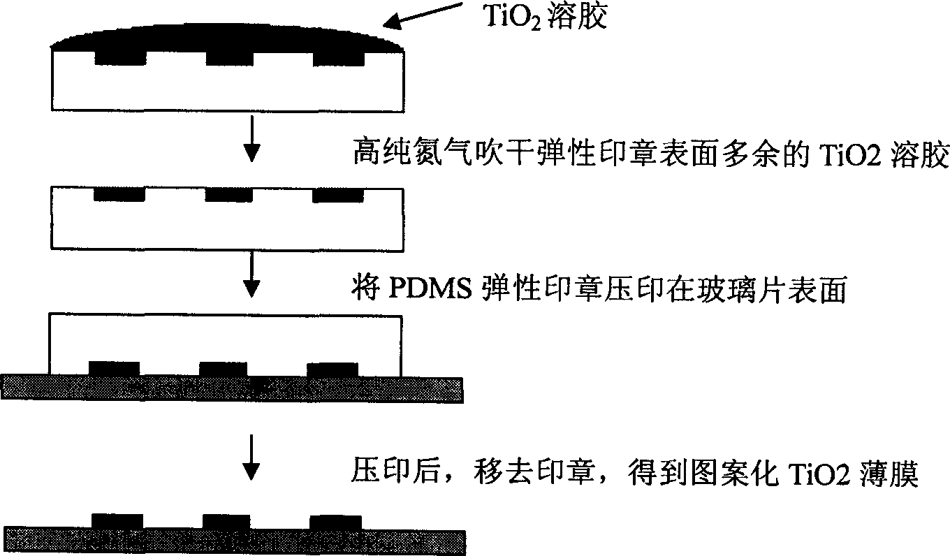
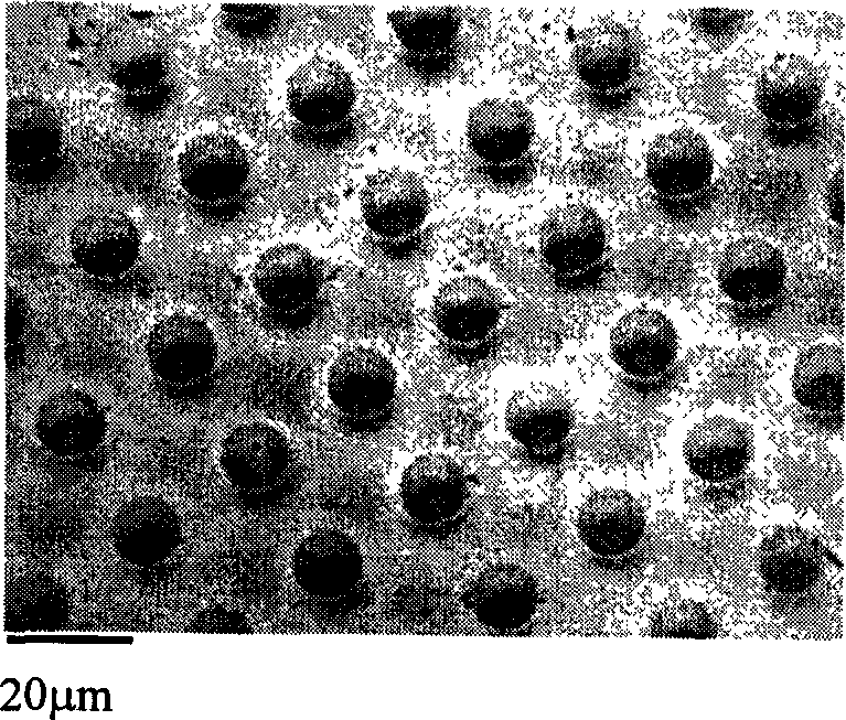
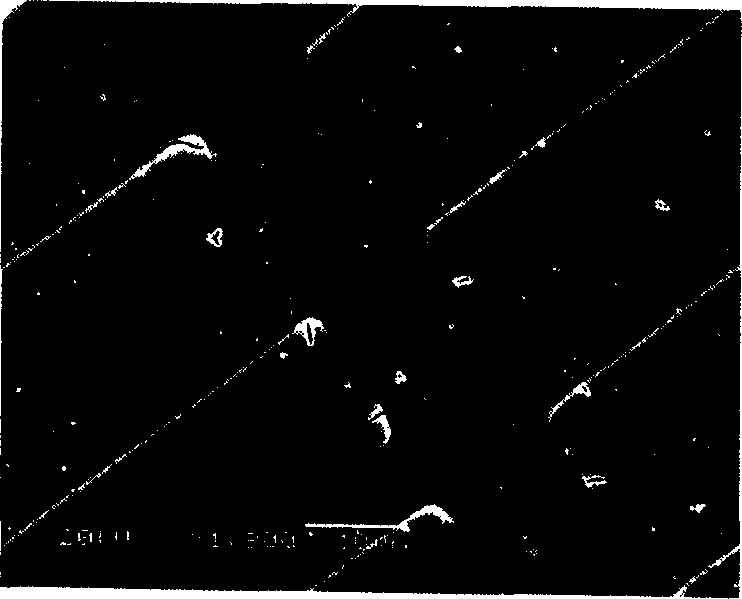
Examples
Embodiment 1
[0016] Fabrication of patterned titania microstructures on ordinary glass slides:
[0017] 1. Pretreatment of slides
[0018] Ordinary glass slides were cut into appropriate sizes and heat-treated with a mixed solution of concentrated sulfuric acid and hydrogen peroxide (Piranha solution) at 90°C for one hour.
[0019] 2. Preparation of Patterned Elastic Stamps
[0020] Polydimethylsiloxane (Sylgard 184 Dow Corning Company) was poured on the patterned surface of the micro-processed single crystal silicon membrane plate, cured at 150° C. for one hour, and aged and peeled off to obtain a silicone rubber elastic stamp with micropatterns.
[0021] 3. Preparation of titania sol
[0022] Butyl titanate [Ti(OBu) 4 ] as the raw material, accurately measure a certain amount of butyl titanate and dissolve it in absolute ethanol, the volume is two-thirds of the required volume, and add acetylacetone (AcAc) as an inhibitor. Then, under vigorous stirring, a mixed solution of nitric aci...
Embodiment 2
[0029] Fabrication of patterned titania microstructures on single crystal silicon wafers:
[0030] 1. Pretreatment of monocrystalline silicon wafers
[0031] Cut the monocrystalline silicon wafers into appropriate sizes and heat-treat them with a mixed solution of concentrated sulfuric acid and hydrogen peroxide (Piranha solution) at 100°C for one and a half hours.
[0032] 2. Preparation of Patterned Elastic Stamps
[0033] Polydimethylsiloxane (Sylgard 184 Dow Corning Company) was poured on the patterned surface of the micro-processed single crystal silicon membrane plate, cured at 150° C. for one hour, and aged and peeled off to obtain a silicone rubber elastic stamp with micropatterns.
[0034] 3. Preparation of titania sol
[0035] Butyl titanate [Ti(OBu) 4 ] as the raw material, accurately measure a certain amount of butyl titanate and dissolve it in absolute ethanol, the volume is two-thirds of the required volume, and add acetylacetone (AcAc) as an inhibitor. Then,...
PUM
 Abstract
Description
Claims
Application Information