Fabrication method of organic thin-film transistors

Inactive Publication Date: 2011-05-19
METAL INDS RES & DEV CENT
View PDF11 Cites 13 Cited by
  • Summary
  • Abstract
  • Description
  • Claims
  • Application Information

AI Technical Summary

Benefits of technology

[0017]In the fabrication method of the present invention, all the functional layers of the OTFT are fabricated by micro-contact printing. The micro-contact printing operation of this fabrication method does not require clean-room environment. The pre-wetting technique employed in the micro-contact printing solves the problem of 2D shrinkage of the printed

Problems solved by technology

The process is complex and costly, unsuitable for mass production.
In the conventional fabrication process of an OTFT, since techniques such as thermal oxide growth in a high-temperature oxidation furnace or chemical vapor deposition (CVD) are used, the whole process is a high-temperature process, which is not suitable for fabricating an OTFT element on a flexible substrate, thereby limiting its application to flexible electronics.
Alt

Method used


Image

  • Fabrication method of organic thin-film transistors
  • Fabrication method of organic thin-film transistors
  • Fabrication method of organic thin-film transistors

Examples


Embodiment Construction

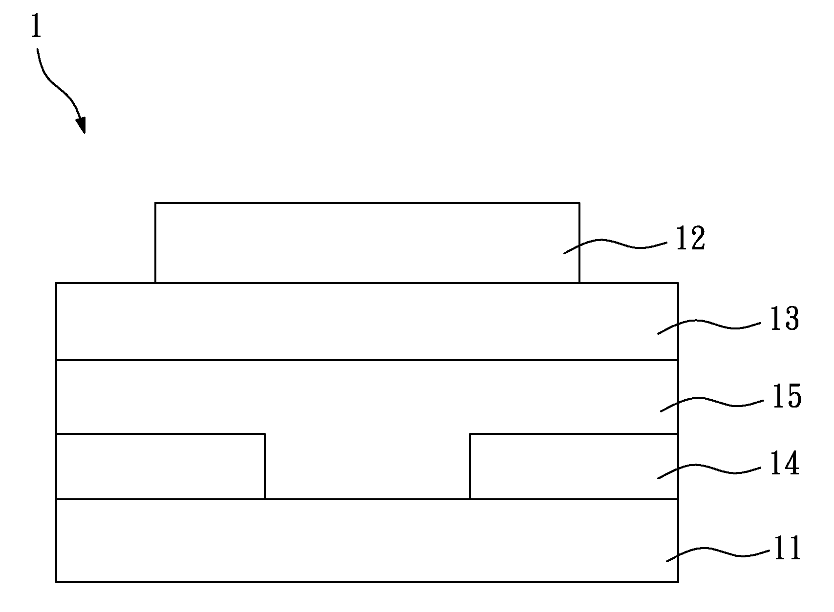
[0023]FIG. 1 is a schematic view of an OTFT according to the present invention. In the fabrication method of OTFTs of the present invention, an organic gate layer 12, an organic dielectric layer 13, an organic source / drain electrode layer 14, and an organic semiconductor layer 15 are formed on a substrate 11 by micro-contact printing, so as to form an OTFT 1. In this embodiment, the substrate 11 is a flexible or rigid substrate, and may be made of polyethylene terephthalate (PET), polycarbonate (PC), polyimide (PI), polyethylene naphthalate (PEN), polyethersulfone (PES), glass, silicon (Si), copper (Cu), or gold (Au). When a metallic substrate is used, there should be an insulation layer before fabrication of the OTFTs.

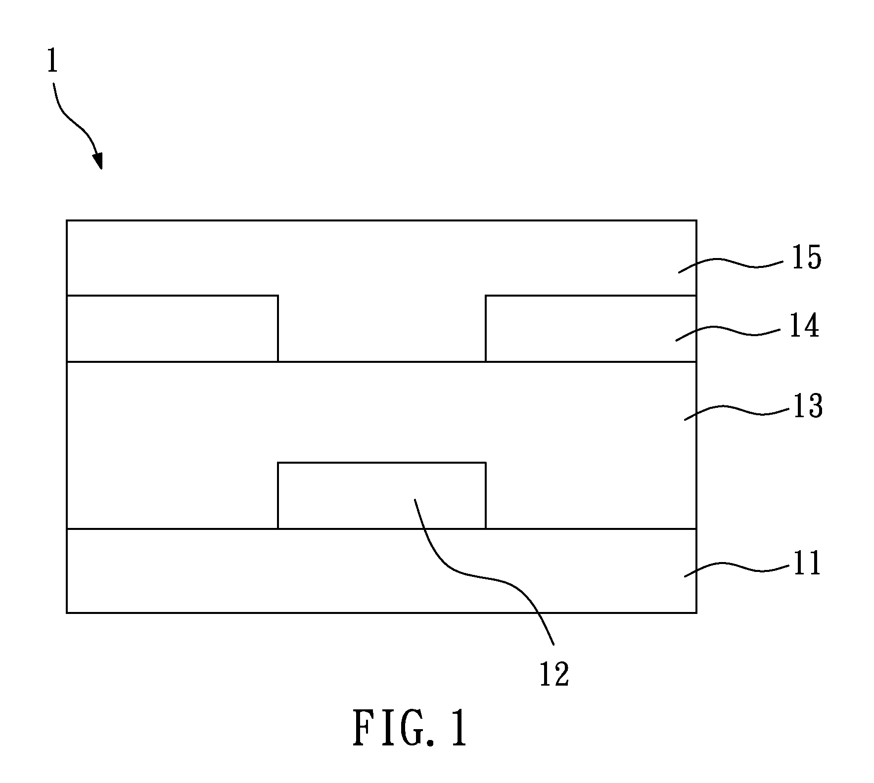
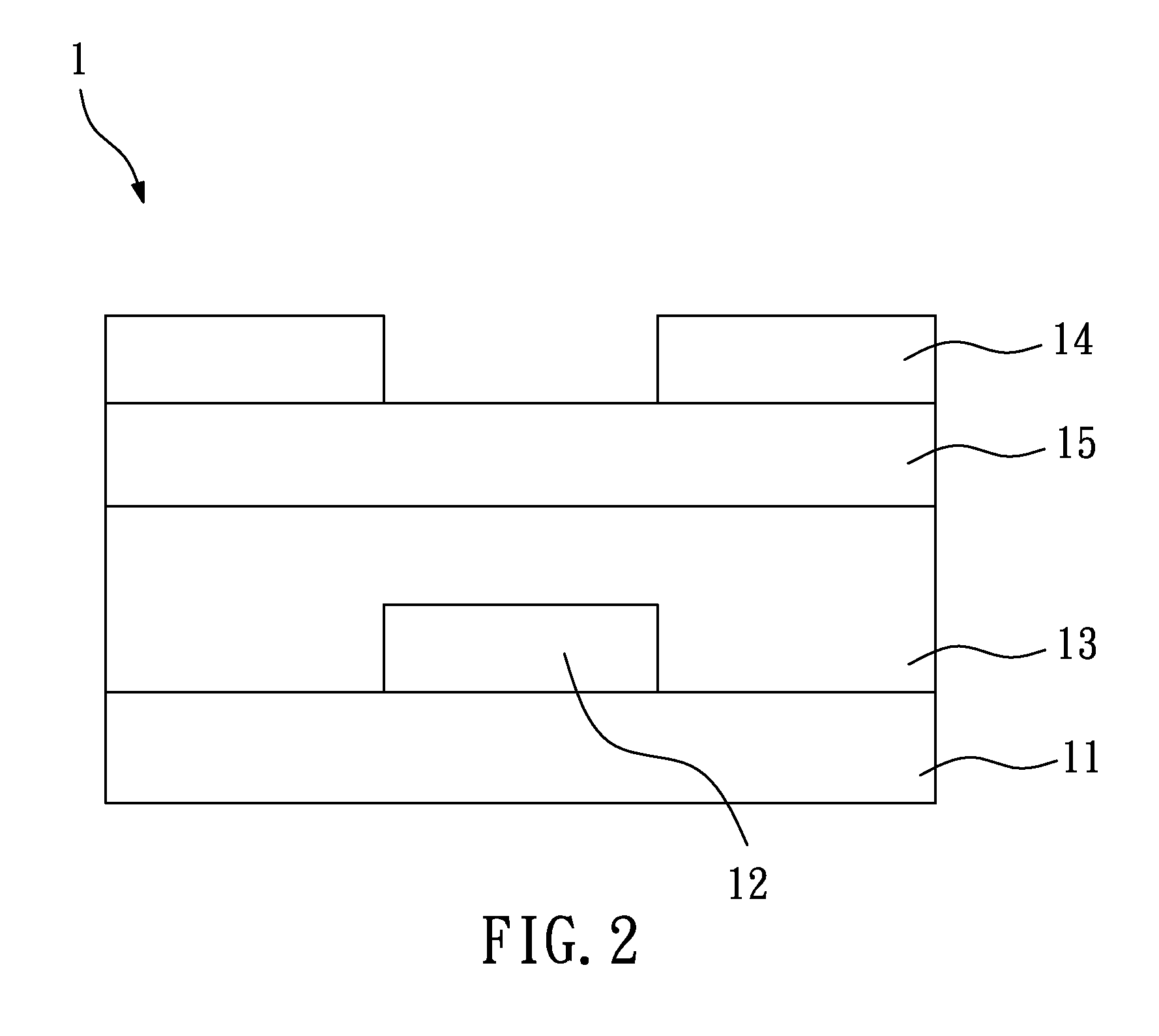
[0024]In this embodiment, the organic gate layer 12, the organic dielectric layer 13, the organic source / drain electrode layer 14, and the organic semiconductor layer 15 are sequentially formed on the substrate 11, so the OTFT 1 is a bottom-gate OTFT (as shown in FIG....


PUM


Abstract

This invention discloses a fabrication method of organic thin-film transistors (OTFTs) using the micro-contact printing. The OTFT can be of the bottom-gate or top-gate configuration. The micro-contact printing operation of this fabrication method does not require clean-room environment and high processing temperature, and does not have the problem of 2D shrinkage of the printed patterns either. Furthermore, the pre-wetting technique employed in the micro-contact printing results in improved fidelity in the pattern transfer and solves the problems of pairing and cross-talking between neighboring patterns.

Description

BACKGROUND OF THE INVENTION[0001]1. Field of the Invention[0002]The present invention relates to a fabrication method of organic thin-film transistors (OTFTs), and more particularly, to a fabrication method of OTFTs using micro-contact printing.[0003]2. Description of the Related Art[0004]A conventional fabrication method of organic thin-film transistors (OTFTs) uses an inorganic substrate like silicon and forms required patterns by masking, exposure, development, and etching in a high vacuum, clean-room environment at high processing temperature. The process is complex and costly, unsuitable for mass production. In recent years, with the emergence of flexible electronics and advances in material technologies, direct coating methods for patterned organic thin films in a non-vacuum environment are developed to replace this conventional method for the fabrication of OTFTs. The results are much simpler, non-vacuum fabrication processes suitable for mass production.[0005]Take silicon su...

Claims


Application Information

Patent Timeline
IPC IPC(8): H01L51/40
CPCH01L51/0004H01L51/0545H01L51/0541H10K71/13H10K10/466H10K10/464
Inventor CHENG, JUNG-WEI JOHNCHEN, CHANG-PENLIN, YEH-MINLEE, CHUN-YIHO, JENG-RONG
Owner METAL INDS RES & DEV CENT
Why Eureka
Try Eureka