Novel detection system

a detection system and nano-array technology, applied in the field of nano-array making methods, can solve the problems of difficult imaging and detection of single monolayers of materials or analytes at a flat surface, limited imaging and detection quality, and only effective imaging

Inactive Publication Date: 2010-02-04
UNIV OF STRATHCLYDE
View PDF11 Cites 4 Cited by
  • Summary
  • Abstract
  • Description
  • Claims
  • Application Information

AI Technical Summary

Benefits of technology

[0015]Another advantage of the present invention is the ability to write features which are closer together than the diffraction limit. Thus, it is possible to write features using DPN, at

Problems solved by technology

Imaging and detection of single monolayers of a material or analyte at a flat surface is difficult.
In the case of analysis by lateral force microscopy (LFM), imaging can only be effectively carried out where the sur

Method used


Image

  • Novel detection system
  • Novel detection system
  • Novel detection system

Examples


Embodiment Construction

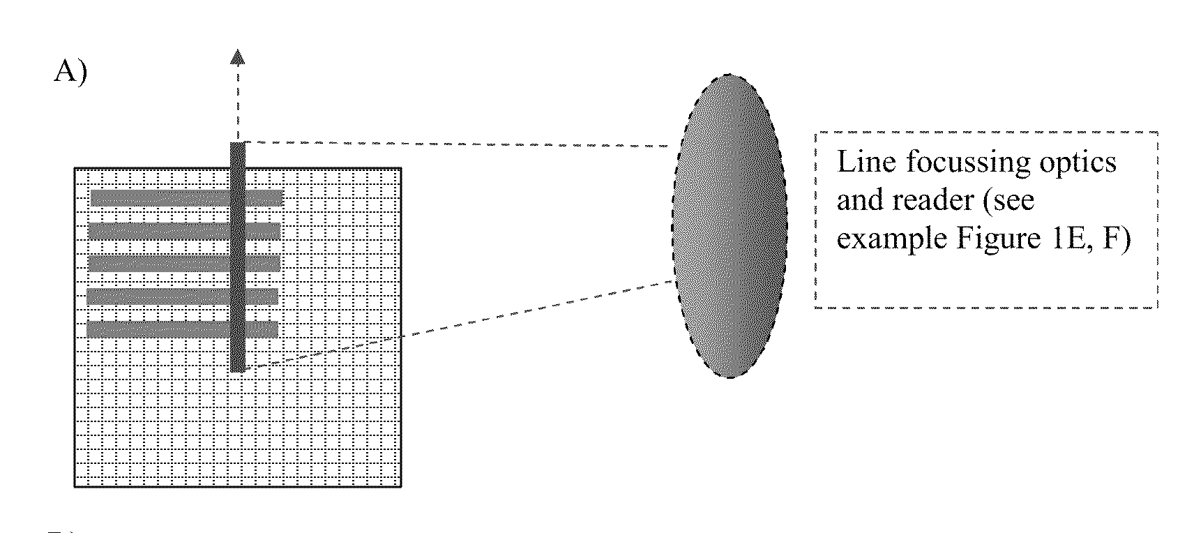
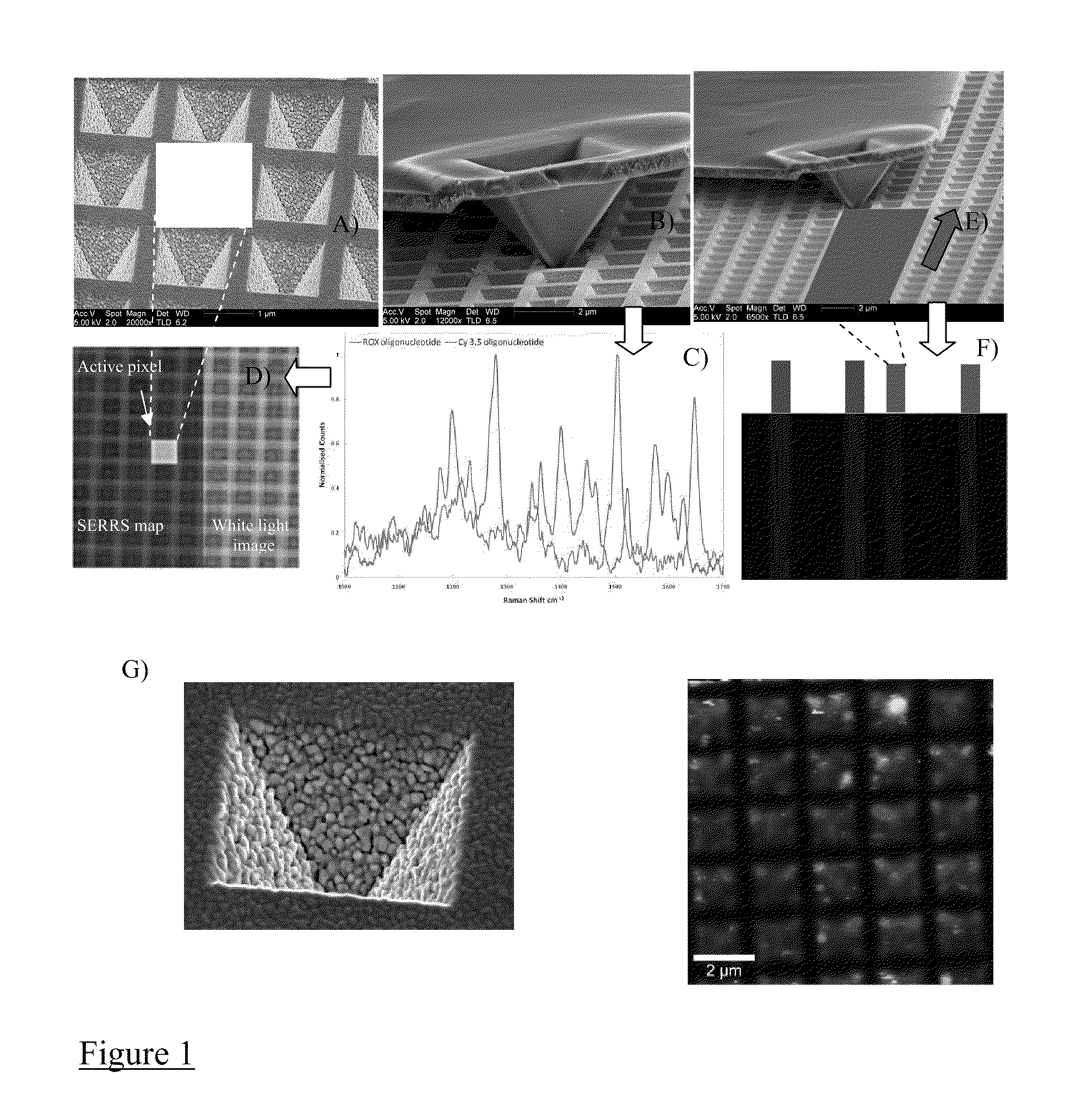
[0044]The inventors show that DPN can be performed accurately in single plasmonic microwells. Furthermore, they have shown that the SE(R)RS readout of these single microwell array dots can be read in isolation by fast line scanning (see FIGS. 1B, C and D) or excited remotely from a point close to but not exactly on the collection point (when collecting in a confocal or semi-confocal set-up.)

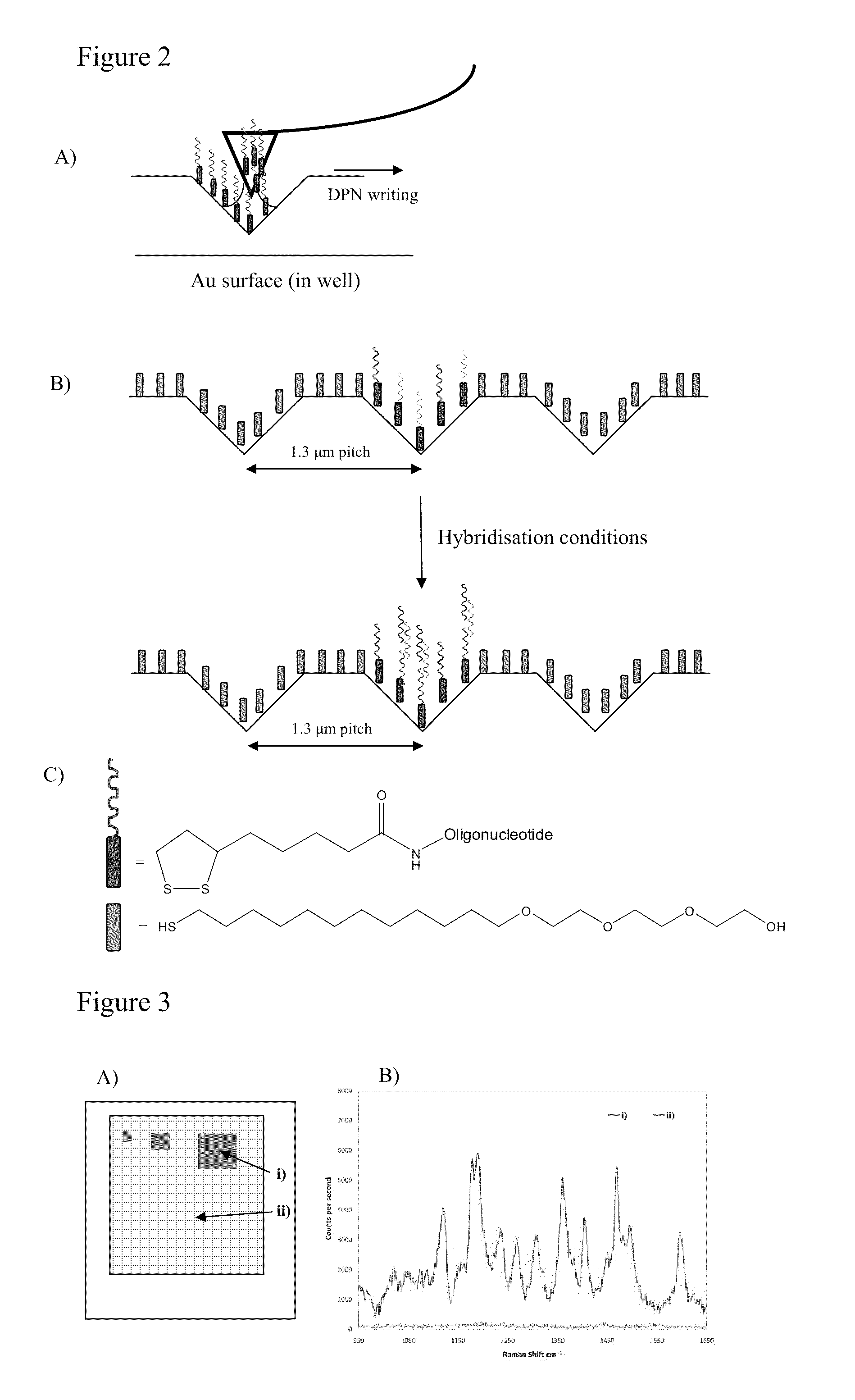
[0045]The inventors also show that it is possible to write lines of material onto non-flat nanostructured surfaces using suitable cantilevers and methods.

1) DPN SERS Array Fabrication:

[0046]The lithography method differs according to the type of SE(R)RS surface used. For example, nanostructured gold surfaces of the type detailed by Perney and co-workers[13] (and shown in FIG. 1A) rely on a inverse pyramid structure with topography and spatial features on the microscale (˜1.3 μm pitch). This design feature is necessary to create surface plasmon resonances and areas of strong electric field (necess...


PUM


Abstract

The present invention relates to methods of making nanoarrays for use in detecting species formed on the surface of the array using SE(R)RS. The methods can involve nanolithographic printing of a compound by dip pen nanolithographic printing. A SE(R)RS substrate can be used for the array and which can be selected from surfaces roughened by the oxidation-reduction cycle (ORC), island films, colloidal nanoparticles and surface-confined nanostructures. A coating or intermediate layer, such as a layer formed of nitrocellulose, can be provided between the compound and the SE(R)RS substrate. There are also provided arrays themselves and methods of using such arrays.

Description

CROSS REFERENCE TO RELATED APPLICATIONS[0001]This applications claims benefit of U.S. Provisional Application No. 61 / 057,558, filed May 30, 2008, which is hereby incorporated herein in its entirety by reference.FIELD OF THE INVENTION[0002]The present invention relates to methods of making nanoarrays using dip pen nanolithography for use in detecting species formed on the surface of the array using SE(R)RS. There are also provided arrays themselves and methods of using such arrays.BACKGROUND OF THE INVENTION[0003]This invention spans the fields of nanotechnology and optical science. More particularly, it concerns the fields of nanolithography especially Dip-Pen Nanolithography (DPN) and the optical technique of surface enhanced Raman scattering (SERS). Dip-Pen Nanolithography (DPN), is a versatile technique in which a scanning probe microscope tip can be used to deliver a material (“ink”) to a surface via a water meniscus. DPN allows controlled deposition of suitable materials conven...

Claims


Application Information

Patent Timeline
IPC IPC(8): G01N33/53B05D5/00G01N21/62
CPCG01N21/658G01N33/6803G01N33/54373C12Q1/00
Inventor STOKES, ROBERTGRAHAM, DUNCAN
Owner UNIV OF STRATHCLYDE
Why Eureka
Try Eureka