Photovoltaic device

a photovoltaic and energy conversion technology, applied in the field of energy conversion devices, can solve the problems of uneven resistance distribution, low durability and photoelectric conversion efficiency of devices using transparent conductive materials, and inability to chemically and mechanically durable,

Inactive Publication Date: 2009-10-22
TSINGHUA UNIV +1
View PDF29 Cites 8 Cited by
  • Summary
  • Abstract
  • Description
  • Claims
  • Application Information

AI Technical Summary

Benefits of technology

[0007]What is needed, therefore, is a photovoltaic device that is more efficient and durable.

Problems solved by technology

However, ITO material has drawbacks, for example, ITO is known not to be chemically and mechanically durable, and as having uneven distribution of resistance.
As a result, the durability and the photoelectric conversion efficiency are relatively low for devices using transparent conductive materials such as ITO.

Method used


Image

  • Photovoltaic device
  • Photovoltaic device
  • Photovoltaic device

Examples


Embodiment Construction

[0014]Reference will now be made to the drawings to describe embodiments of the present photovoltaic device in detail.

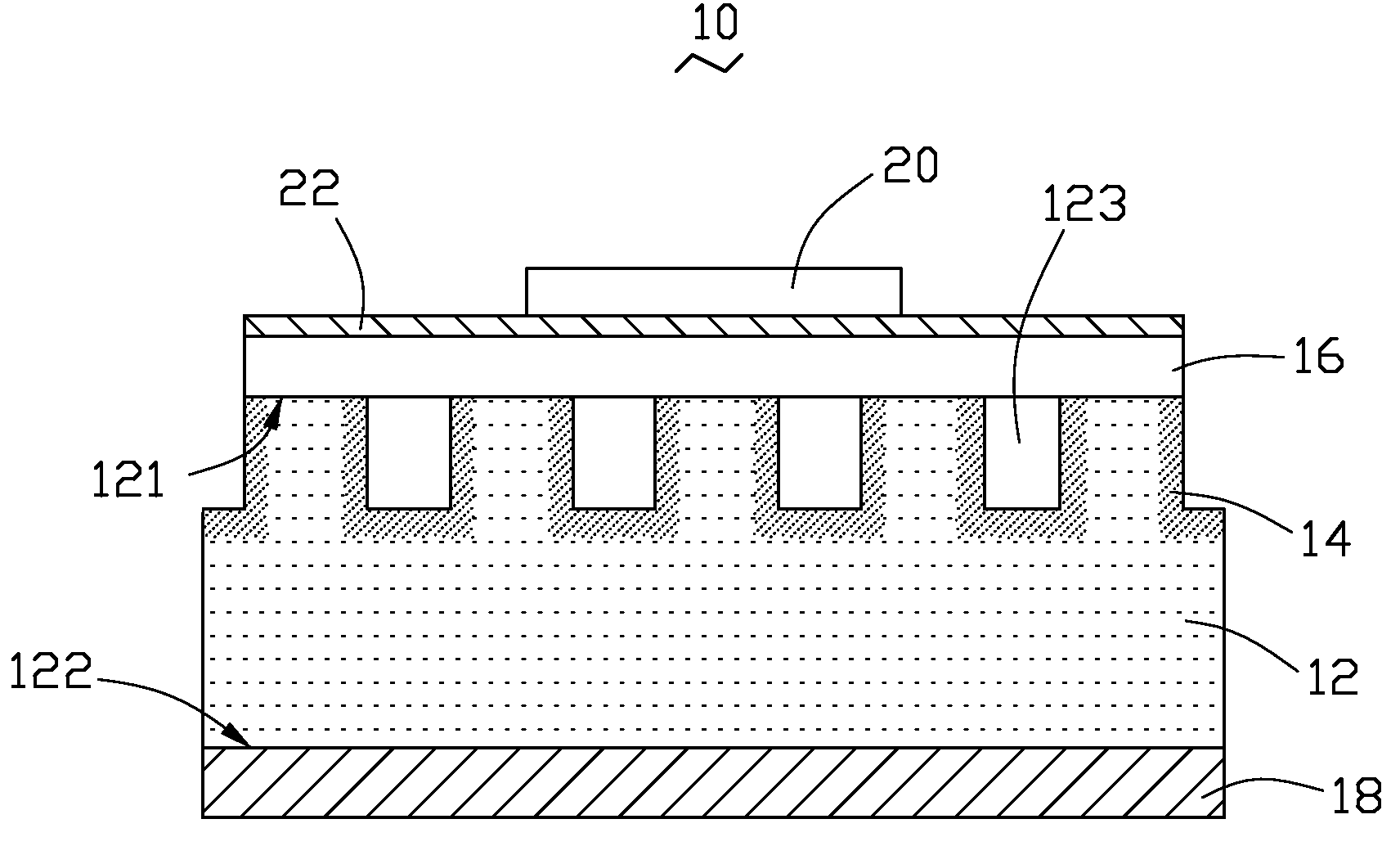
[0015]Referring to FIG. 1, a photovoltaic device 10 according to an exemplary embodiment, is shown. The photovoltaic device 10 includes a substrate 12, a doped layer 14, a first electrode 16, and a second electrode 18.

[0016]The substrate 12 can be made of single crystal silicon. In the exemplary embodiment, the substrate 12 is p-type single crystal silicon. In addition, a thickness of the substrate 12 is in a range from about 200 μm to about 300 μm. The substrate 12 has a front surface 121 and a rear surface 122, as shown in FIG. 1. The front surface 121 of the substrate 12 defines a plurality of cavities 123. That is, some portions of the front surface 121 form the cavities 123 for enhancing light collation and increasing the area of p-n junction formation. The cavities 123 are distributed evenly and are spaced from each other by a distance in a range from about 10 ...


PUM

PropertyMeasurementUnit
thicknessaaaaaaaaaa
distanceaaaaaaaaaa
depthaaaaaaaaaa

Abstract

A photovoltaic device includes a substrate, a doped layer, a first electrode and a second electrode. The substrate has a plurality of cavities defined therein. The doped layer is in contact the substrate. The first electrode including a carbon nanotube composite material is adjacent to the substrate. The second electrode is attached to the substrate.

Description

BACKGROUND[0001]1. Technical Field[0002]The invention relates to energy conversion devices, and particularly to a photovoltaic device.[0003]2. Description of Related Art[0004]Currently, solar energy is considered a renewable and clean alternative energy source. Solar energy is generally produced by photovoltaic cells, also known as solar cells. The solar cell is a device that converts light into electrical energy using the photoelectric effect.[0005]Generally, the solar cell includes a large-area p-n junction made from silicon. Silicon employed in the solar cell can be single crystal silicon or polycrystalline silicon. Referring to FIG. 4, a conventional solar cell 30 according to the prior art generally includes a silicon substrate 32, a doped silicon layer 34, a front electrode 36, and a rear electrode 38. The doped silicon layer 34 is in contact with the silicon substrate 32 to form a p-n junction. The front electrode 36 is disposed on and electrically connected to the doped sili...

Claims


Application Information

Patent Timeline
Patent Type & Authority Applications(United States)
IPC IPC(8): H01L31/00
CPCB82Y20/00G02B6/1226H01L31/022425Y02E10/547H01L31/0236H01L31/03529H01L31/068H01L31/022466
Inventor SUN, HAI-LINJIANG, KAI-LILI, QUN-QINGFAN, SHOU-SHAN
Owner TSINGHUA UNIV
Why Eureka
Try Eureka