
Eureka
For R&D, Eureka makes reading and utilizing patents & technical documents easy.
Eureka AIR
Designed for self-driven R&D workflows. Generate viable solutions, solve complex R&D challenges, empower your innovation with AI.

Eureka Materials
Designed for material experts only. Revolutionize your material R&D, from search, analyze, to developing new materials.

TechResearch
Generate reliable direction feasibility study reports for your R&D in just a few steps.

TechSeek
Discover and master advanced knowledge NOW. Basics, ideas, possibilities, all at once.

TechMind
As an expert in R&D Theories, TechMind can generates customized viable solutions instantly.

TechRisk
Analyze your overall solution with one click, know your potential R&D risks in advance.

TechMonitor
Get weekly tech updates, stay abreast of the latest tech innovations and key insights.
Magnetron sputtering apparatus and production method of thin film
- Summary
- Abstract
- Description
- Claims
- Application Information
AI Technical Summary
Benefits of technology
Problems solved by technology
Method used
Image

Examples
Embodiment Construction
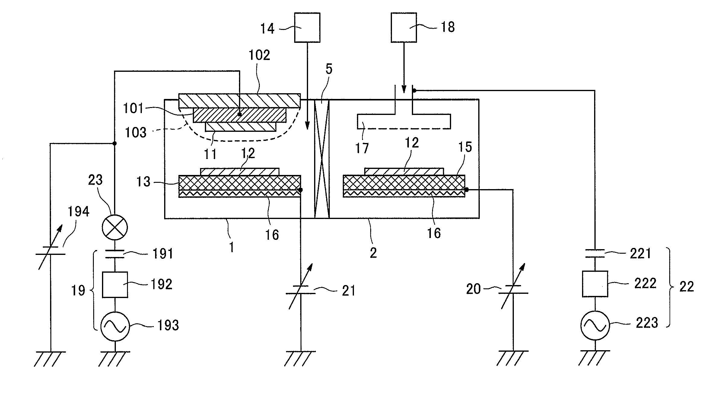
[0027]FIG. 1 is a schematic view of the apparatus according to a first example of the present invention. Reference numeral 1 is a first chamber, 2 is a second chamber (annealing unit) vacuum-connected to the first chamber 1, 3 is a substrate charging chamber, 4 is a discharging chamber, 5 is a gate valve, 11 is a target using a boron-lanthanum compound such as LaB6, 12 is a substrate, 13 is a substrate holder (first substrate holder) for holding the substrate 12, 14 is a sputtering gas feed system, 15 is a substrate holder (second substrate holder), 16 is a heating mechanism, 17 is a plasma electrode, 18 is a gas feed system for a plasma source, 19 is a sputtering high-frequency power source system, 101 is a cathode capable of attaching the target 11 configured of a boron-lanthanum compound containing boron and lanthanum atoms, 102 is a magnetic field generation device, 103 is a magnetic-field region, 191 is a blocking capacitor, 192 is a matching circuit, 193 is a high-frequency po...
PUM
| Property | Measurement | Unit |
|---|---|---|
| Power | aaaaa | aaaaa |
| Vacuum | aaaaa | aaaaa |
Abstract
Description
Claims
Application Information
 - R&D Engineer
- R&D Manager
- IP Professional
- Industry Leading Data Capabilities
- Powerful AI technology
- Patent DNA Extraction
Browse by: Latest US Patents, China's latest patents, Technical Efficacy Thesaurus, Application Domain, Technology Topic, Popular Technical Reports.
© 2024 PatSnap. All rights reserved.Legal|Privacy policy|Modern Slavery Act Transparency Statement|Sitemap|About US| Contact US: help@patsnap.com