Composite transfer gate and fabrication thereof

Inactive Publication Date: 2009-10-22
UNITED MICROELECTRONICS CORP
View PDF28 Cites 10 Cited by
  • Summary
  • Abstract
  • Description
  • Claims
  • Application Information

AI Technical Summary

Benefits of technology

[0007]Accordingly, this invention provides a composite transfer gate, which may be applied to a transfer transistor of an el

Problems solved by technology

It is difficult to make the dark current inhibition and image lag prevention both effective with a fully N-doped transfer gate.
However, in such a case, the threshold voltage under a portion of th

Method used


Image

  • Composite transfer gate and fabrication thereof
  • Composite transfer gate and fabrication thereof
  • Composite transfer gate and fabrication thereof

Examples


Embodiment Construction

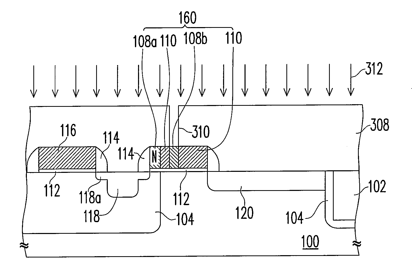
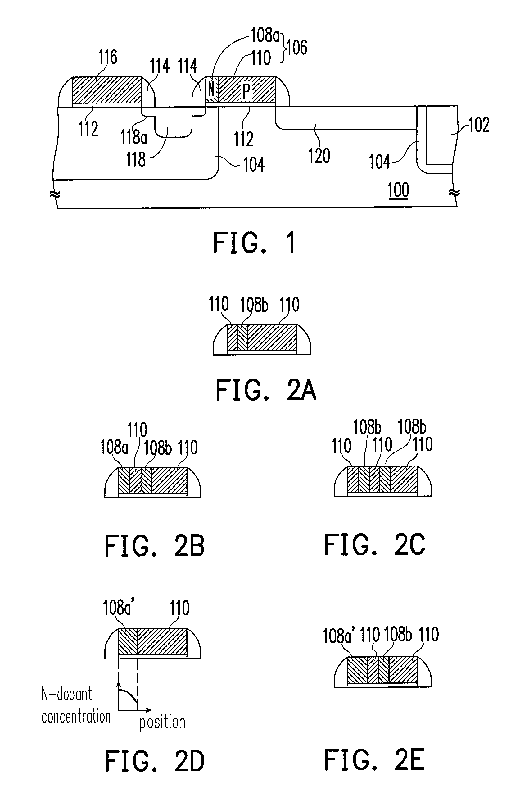
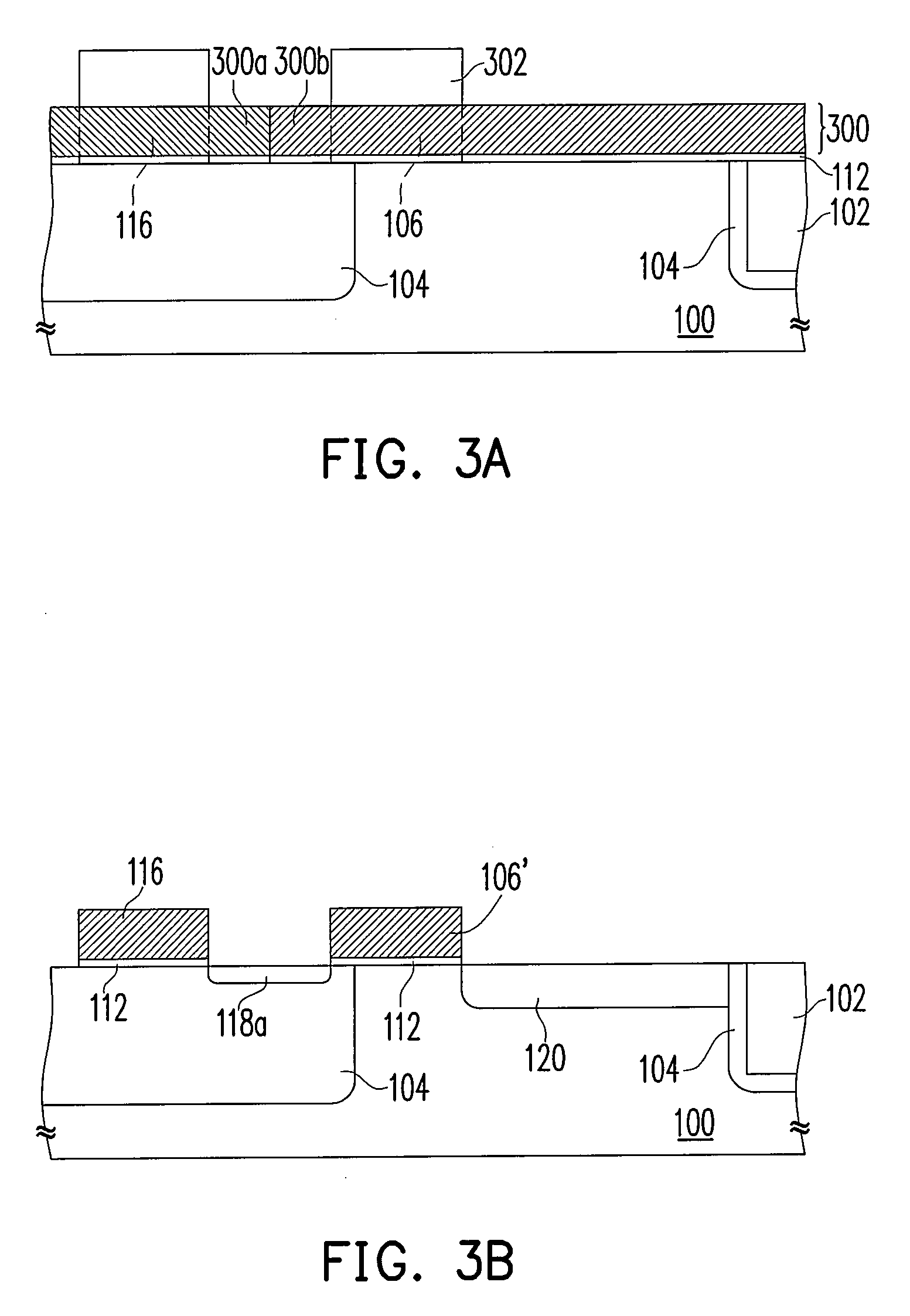
[0027]FIG. 1 illustrates a local cross-sectional view of a CMOS image sensor unit that includes a composite transfer gate according to an embodiment of this invention. The CMOS image sensor is a kind of optical sensor.

[0028]Referring to FIG. 1, in a semiconductor substrate 100, an isolation layer 102, a P-type field doped region 104 around the isolation layer 102, an N-doped region 118 as the floating node and an N-doped region 120 as the electron reservoir are formed. The composite transfer gate 106 is disposed over the substrate 100 between the floating node 118 and the electron reservoir 120, including a P-type portion 110 and an N-type portion 108a at an edge thereof facing the floating node 118 and being separated from the substrate 100 by a gate dielectric layer 112. The doped region 104 extends to under the N-type portion 108a. The width of the N-type portion 108a is preferably less than 0.15 μm. When the width of the composite transfer gate 106 is more than 0.45 μm, the widt...


PUM


Abstract

A composite transfer gate is described, which is disposed over a semiconductor substrate between an electron reservoir and a floating node in the semiconductor substrate. The composite transfer gate includes at least one N-type portion and a P-type portion that are arranged laterally.

Description

BACKGROUND OF THE INVENTION[0001]1. Field of Invention[0002]This invention relates to a semiconductor structure and fabrication thereof, and more particularly relates to a composite transfer gate disposed between an electron reservoir and a floating node and to a method of fabricating the same.[0003]2. Description of Related Art[0004]The combination of an electron reservoir, a floating node and a transfer gate between them is frequent seen in various kinds of signal sensors, for example, a CMOS image sensor (CIS). Each pixel of a CIS is usually disposed with four MOS transistors including the transfer transistor.[0005]In a traditional CIS, a transfer gate is fully N-doped like the floating node, while an extra pinning region of P-type is formed under the transfer gate and in the electron reservoir to reduce the dark current, so that the full well capacity of photoelectrons is decreased lowering the S / N ratio of the sensor. It is difficult to make the dark current inhibition and imag...

Claims


Application Information

Patent Timeline
IPC IPC(8): H01L31/00H01L21/00
CPCH01L21/82345H01L21/823842H01L27/14689H01L27/14643H01L27/14603
Inventor SZE, JHY-JYI
Owner UNITED MICROELECTRONICS CORP
Why Eureka
Try Eureka