Through-electrode, circuit board having a through-electrode, semiconductor package having a through-electrode, and stacked semiconductor package having the semiconductor chip or package having a through-electrode
- Summary
- Abstract
- Description
- Claims
- Application Information
AI Technical Summary
Benefits of technology
Problems solved by technology
Method used
Image

Examples
Embodiment Construction
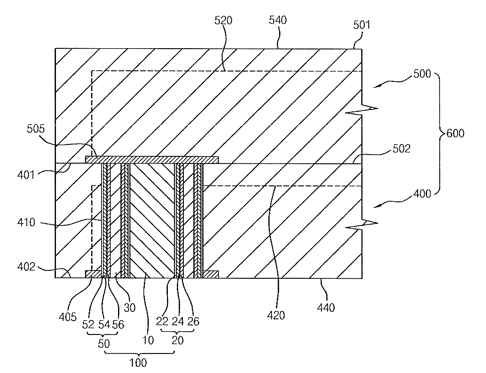
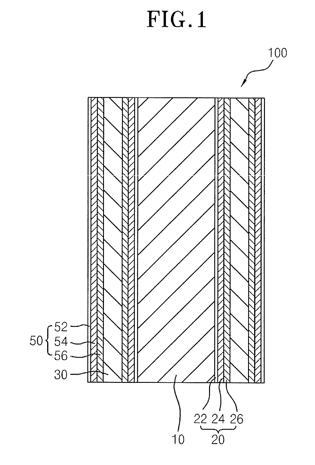
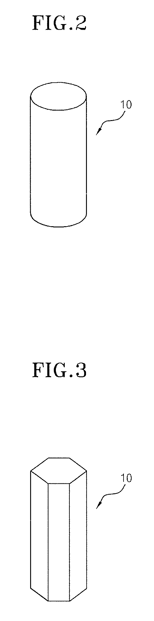
[0037]Two or more semiconductor memory chips, or two or more semiconductor packages having the multiple chips stacked therein, or even a combination of chips and packages can be stacked in a semiconductor package. The stacked components in a package are electrically connected to each other. Hereinafter, any of the permissible stacked components will be referred to as a “semiconductor chip” which term shall mean not only the semiconductor memory chip but also any other memory components that are packageable in a semiconductor package either presently or foreseeably. According to the present invention, a through-hole is formed in each of the stacked semiconductor chips, and a through-hole electrode is formed inside the through-holes to provide electrical connection between the stacked semiconductor chips.
[0038]To form a through-electrode inside the through-holes, a metal (such as copper) plating or a solder reflow technique may be used. However, using a metal plating process to form a...
PUM
 Abstract
Description
Claims
Application Information
 - Generate Ideas
- Intellectual Property
- Life Sciences
- Materials
- Tech Scout
- Unparalleled Data Quality
- Higher Quality Content
- 60% Fewer Hallucinations
Browse by: Latest US Patents, China's latest patents, Technical Efficacy Thesaurus, Application Domain, Technology Topic, Popular Technical Reports.
© 2025 PatSnap. All rights reserved.Legal|Privacy policy|Modern Slavery Act Transparency Statement|Sitemap|About US| Contact US: help@patsnap.com