Time resolved radiation assisted device alteration

Inactive Publication Date: 2009-10-22
NXP USA INC
View PDF9 Cites 14 Cited by
  • Summary
  • Abstract
  • Description
  • Claims
  • Application Information

AI Technical Summary

Problems solved by technology

These problem areas are “suspect locations” which includes performance limiting areas or defective circuits and the like.
A timing adjustment may reveal, for example, a race condition between two or more circuit paths thereby limiting maximum frequency of operation of the semiconductor device.
The test pattern generally includes hundreds or thousands (or more) of test vectors, so that selection of timing is a time-consuming trial and error approach.
The TRLEM procedure without timing information often consumes a significant amount of analysis time with a relatively low success rate (e.g., success rate is estimated to be less than 1 percent).
Probe selection is particularly difficult since only one probe point is monitored at a time over a very small window of time relati

Method used


Image

  • Time resolved radiation assisted device alteration
  • Time resolved radiation assisted device alteration
  • Time resolved radiation assisted device alteration

Examples


Embodiment Construction

[0018]The following description is presented to enable one of ordinary skill in the art to make and use the present invention as provided within the context of a particular application and its requirements. Various modifications to the preferred embodiment will, however, be apparent to one skilled in the art, and the general principles defined herein may be applied to other embodiments. Therefore, the present invention is not intended to be limited to the particular embodiments shown and described herein, but is to be accorded the widest scope consistent with the principles and novel features herein disclosed.

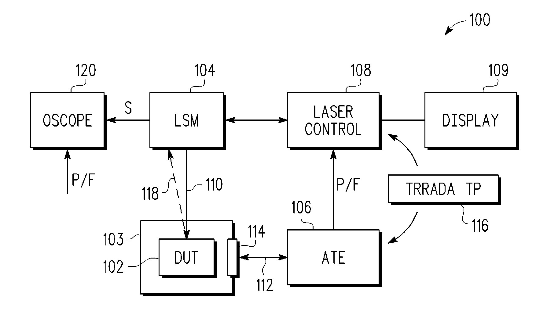
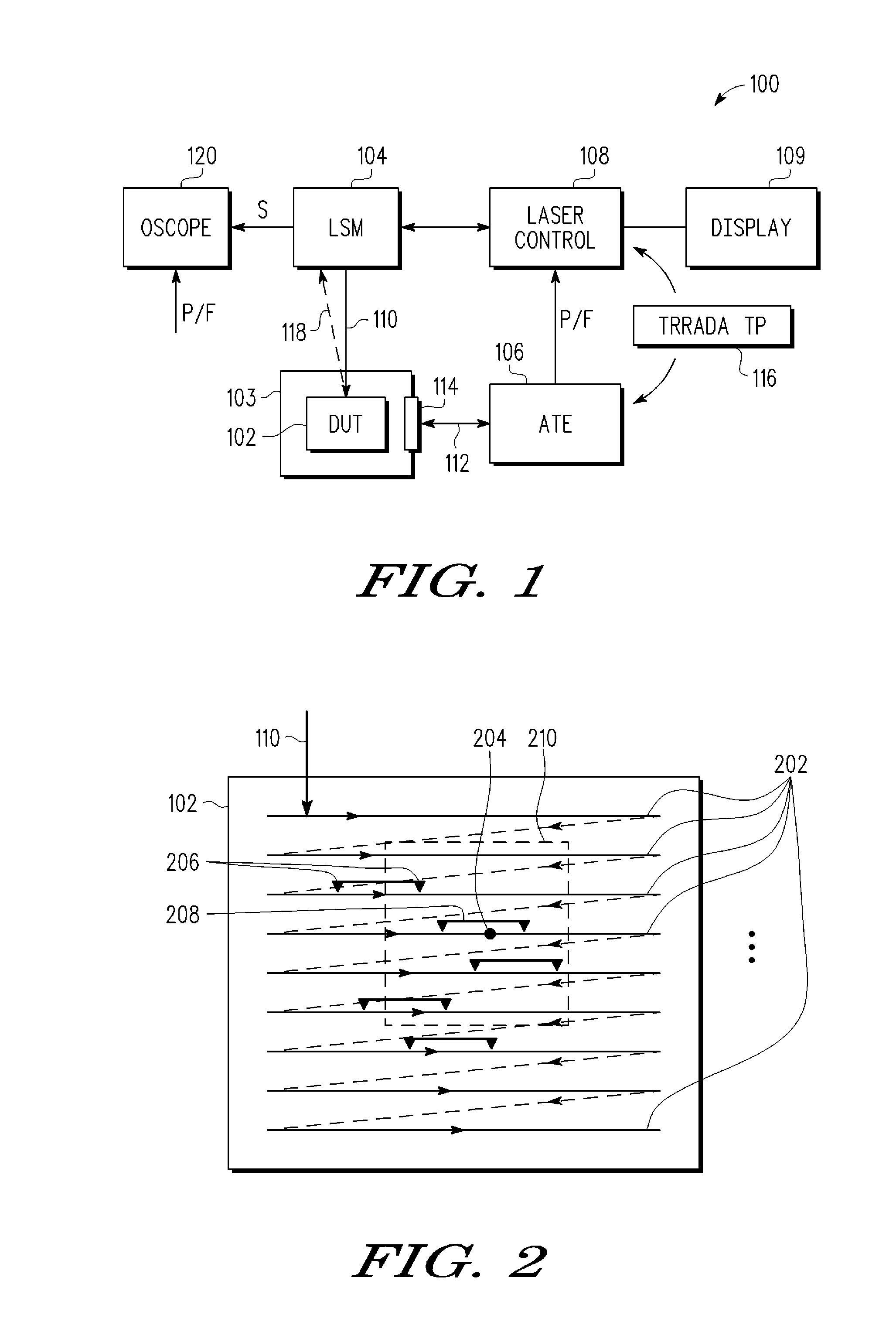
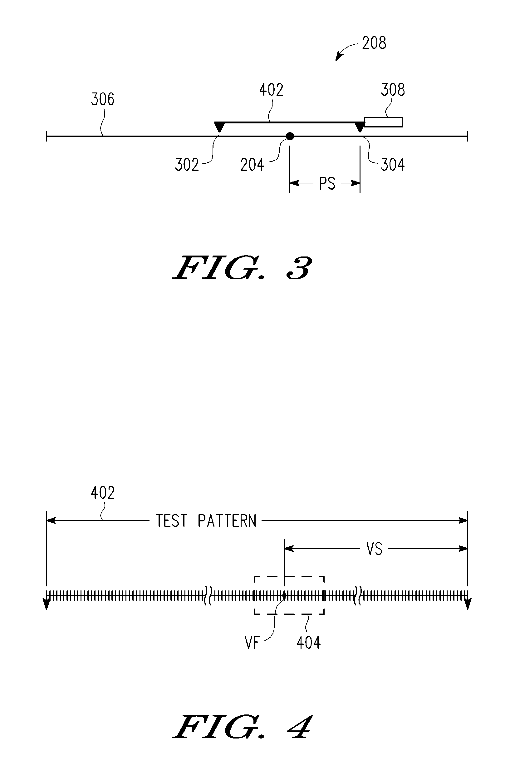
[0019]FIG. 1 is a simplified block diagram of a time resolved laser assisted device alteration (TRLADA) test system 100 implemented according to an exemplary embodiment for testing a semiconductor device under test (DUT) 102. The TRLADA test system 100 is implemented according to one embodiment of the time resolved radiation assisted device alteration described herein, in which...


PUM


Abstract

A method of time resolved radiation assisted device alteration testing of a semiconductor circuit which includes performing spatially resolved radiation assisted circuit testing on the semiconductor circuit while applying a test pattern to determine a pass-fail modulation location, asynchronously scanning the semiconductor circuit with radiation while repeatedly applying the test pattern and providing pass-fail results, combining corresponding pass-fail results provided during the asynchronously scanning to determine a shifted pass-fail modulation indication, determining time shift information between the pass-fail modulation location and the shifted pass-fail modulation indication, and identifying at least one of the test vectors based on the time shift information. The radiation may be a continuous wave laser beam. The time shift information may be determined by scanning an image, incorporating graphics into the image indicating the pass-fail modulation location and the shifted pass-fail modulation indication, and measuring a pixel shift on the scanned image.

Description

BACKGROUND OF THE INVENTION[0001]1. Field of the Invention[0002]The present invention relates in general to identifying sensitive or performance limiting areas or suspect locations of semiconductor devices, and more specifically to a time resolved radiation assisted device alteration technique for determining timing information relative to a test pattern of suspect locations of a device under test using asynchronously scanned radiation stimulation such as a laser.[0003]2. Description of the Related Art[0004]A variety of radiation-based stimulation circuit testing techniques are known for failure or performance analysis of semiconductor devices. Radiation stimulation involves the use of various forms of radiation or emissions or the like with sufficient energy to modify operating behavior of semiconductor circuitry for the purpose of identifying potential problem areas of a semiconductor device. These problem areas are “suspect locations” which includes performance limiting areas or ...

Claims


Application Information

Patent Timeline
IPC IPC(8): G01R31/00
CPCG01R31/2894G01R31/2882
Inventor ERINGTON, KENT B.ASQUITH, JOHN E.
Owner NXP USA INC
Why Eureka
Try Eureka