High voltage CMOS output buffer constructed from low voltage CMOS transistors

Active Publication Date: 2009-10-22
NAT SEMICON CORP
View PDF3 Cites 16 Cited by
  • Summary
  • Abstract
  • Description
  • Claims
  • Application Information

AI Technical Summary

Problems solved by technology

Furthermore, since CMOS device scaling has been progressing at a very rapid rate, VDDINT has also been decreasing at a very rapid rate.
A basic problem, however, is that the standard system power supply voltage VDDSYS has been

Method used


Image

  • High voltage CMOS output buffer constructed from low voltage CMOS transistors
  • High voltage CMOS output buffer constructed from low voltage CMOS transistors
  • High voltage CMOS output buffer constructed from low voltage CMOS transistors

Examples


Embodiment Construction

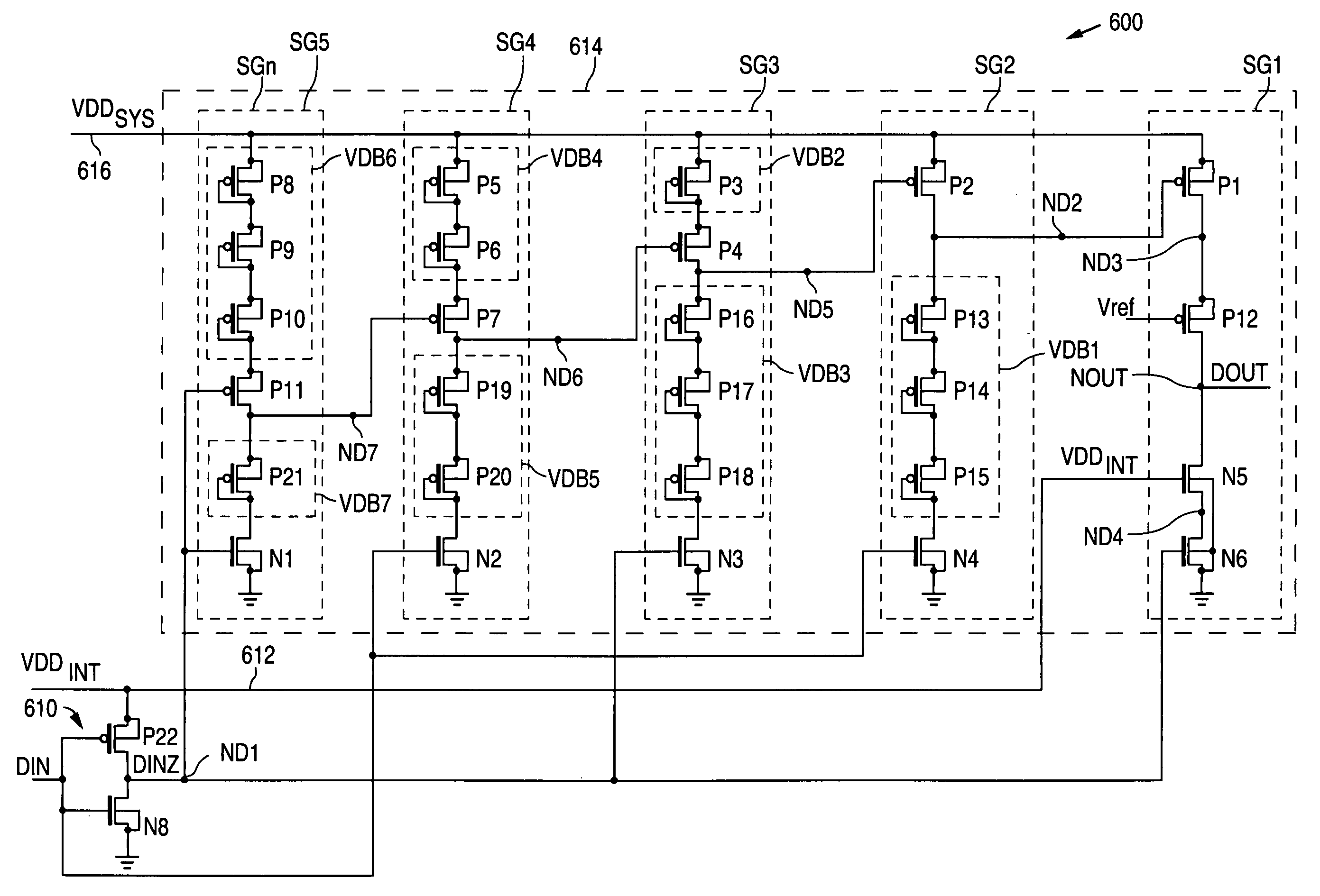
[0042]In accordance with the present invention, FIG. 6 shows a schematic diagram that illustrates an example of a high voltage output buffer 600. As described in greater detail below, output buffer 600 can supply a high voltage output swing using only low voltage CMOS transistors. For example, output buffer 600 can supply a 5V output swing using only 3.3V CMOS transistors, or a 3.3V output swing using only 2.5V CMOS transistors.

[0043]As shown in FIG. 6, output buffer 600 includes an inverter 610 that inverts a low voltage input data signal DIN to generate a low voltage data output signal DINZ. Moreover, inverter 610 includes a PMOS transistor P22 and an NMOS transistor N8. Furthermore, PMOS transistor P22 has a gate connected to receive the low voltage input data signal DIN, a drain connected to an intermediate node ND1, and a source and substrate connected to an internal power supply line 612, which is connected to an internal power supply voltage VDDINT. In addition, NMOS transist...


PUM


Abstract

A high voltage CMOS output buffer is constructed from low voltage CMOS transistors. The output buffer employs a series of unique CMOS inverter stages, each of which contains a switched PMOS transistor, one or more voltage drop blocks, and a switched NMOS transistor. The voltage drop blocks are composed of stacked PMOS transistors that are diode-connected—i.e., the PMOS gate terminal is connected to the PMOS drain terminal, and the PMOS body (N-well) terminal is connected to the PMOS source terminal. The diode-connected PMOS transistors reduce the voltage across the transistor gate oxide to a safe value, for all internal PMOS/NMOS transistors inside the CMOS output buffer.

Description

BACKGROUND OF THE INVENTION[0001]1. Field of the Invention[0002]The present invention relates to CMOS output buffers, and more particularly, to a high voltage CMOS output buffer that is constructed from low voltage CMOS transistors.[0003]2. Description of the Related Art.[0004]CMOS processing rules are being continually scaled downward, producing smaller and faster transistors that have shorter channel lengths and lower threshold voltages. CMOS device scaling also offers other important advantages, including shorter interconnect wires that have lower capacitance, and the use of lower VDD voltages.[0005]The use of lower VDD voltages is extremely important, because it significantly decreases PWRDIG, the digital power dissipation inside the core of a CMOS chip. The formula for calculating PWRDIG is shown in EQ. 1.PWRDIG=C*VDDINT2*F   EQ. 1where C represents the average gate plus interconnect capacitance, VDDINT represents the internal (digital core) power supply voltage, and F represen...

Claims


Application Information

Patent Timeline
IPC IPC(8): H03K3/00
CPCH03K19/00315H03K19/018521
Inventor PASQUALINI, RONALD
Owner NAT SEMICON CORP
Why Eureka
Try Eureka