Apparatus and method for electrostatic discharge protection of a transmit integrated circuit

a technology of integrated circuits and apparatus, applied in the direction of emergency protective circuit arrangements, emergency protection circuit arrangements, etc., can solve the problems of esd damage to structures, signal distortion, and inability to use bond wires to couple chip pads, etc., to ensure minimal distortion of output signals.

Active Publication Date: 2010-08-31
QUALCOMM INC
View PDF6 Cites 13 Cited by
  • Summary
  • Abstract
  • Description
  • Claims
  • Application Information

AI Technical Summary

Benefits of technology

[0009]For a CMOS integrated circuit in a package without bond wires, an electrostatic discharge (ESD) protect block may couple between an input / output (I / O) pad, to which a transmit circuit may couple, and an ESD clamp circuit coupled to ground. The ESD protect block, which may couple to the same I / O pad as the transmit circuit, may be implemented such that the load seen by the transmit circuit is low, thereby ensuring minimal distortion of the output signal. During transmission, one or more capacitors within the ESD protect block may charge up to various levels near the peak transmit voltage, which reverse biases one or more diodes in the ESD protect block, thereby buffering the transmit circuit from the capacitive load of the ESD clamp circuit. The ESD protect block may prevent the ESD clamp circuit from activating due to the high peak voltages output from the transmit circuit.

Problems solved by technology

ESD may damage an unprotected complementary metal oxide semiconductor (CMOS) integrated circuit, and shrinking CMOS process technologies result in structures more susceptible to ESD damage.
Coupling such an ESD clamp circuit directly to an input or output node may provide a large capacitive load to a high frequency input or output signal coupled to the same node, thereby distorting the signal.
Packages without bond wires, such as chip scale packages, however, do not use bond wires to couple the chip pads to the package inputs / output nodes.
The on-chip inductor Loc 204 may isolate the PA 201 from the ESD clamp circuit's 202 capacitance, but disadvantageously, the on-chip inductor Loc 204 may require significant chip area to implement.
Additionally, the resistance of the on-chip inductor Loc 204 may result in an undesirable voltage drop across the inductor Loc 204 during the ESD event, which may compromise the level of ESD protection.

Method used


Image

  • Apparatus and method for electrostatic discharge protection of a transmit integrated circuit
  • Apparatus and method for electrostatic discharge protection of a transmit integrated circuit
  • Apparatus and method for electrostatic discharge protection of a transmit integrated circuit

Examples


Embodiment Construction

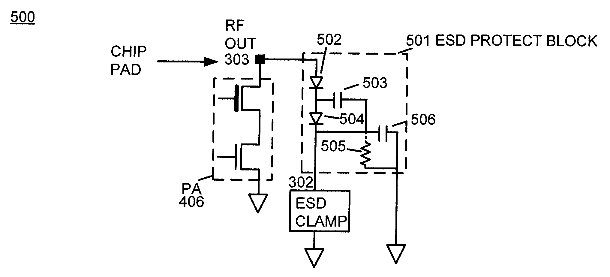
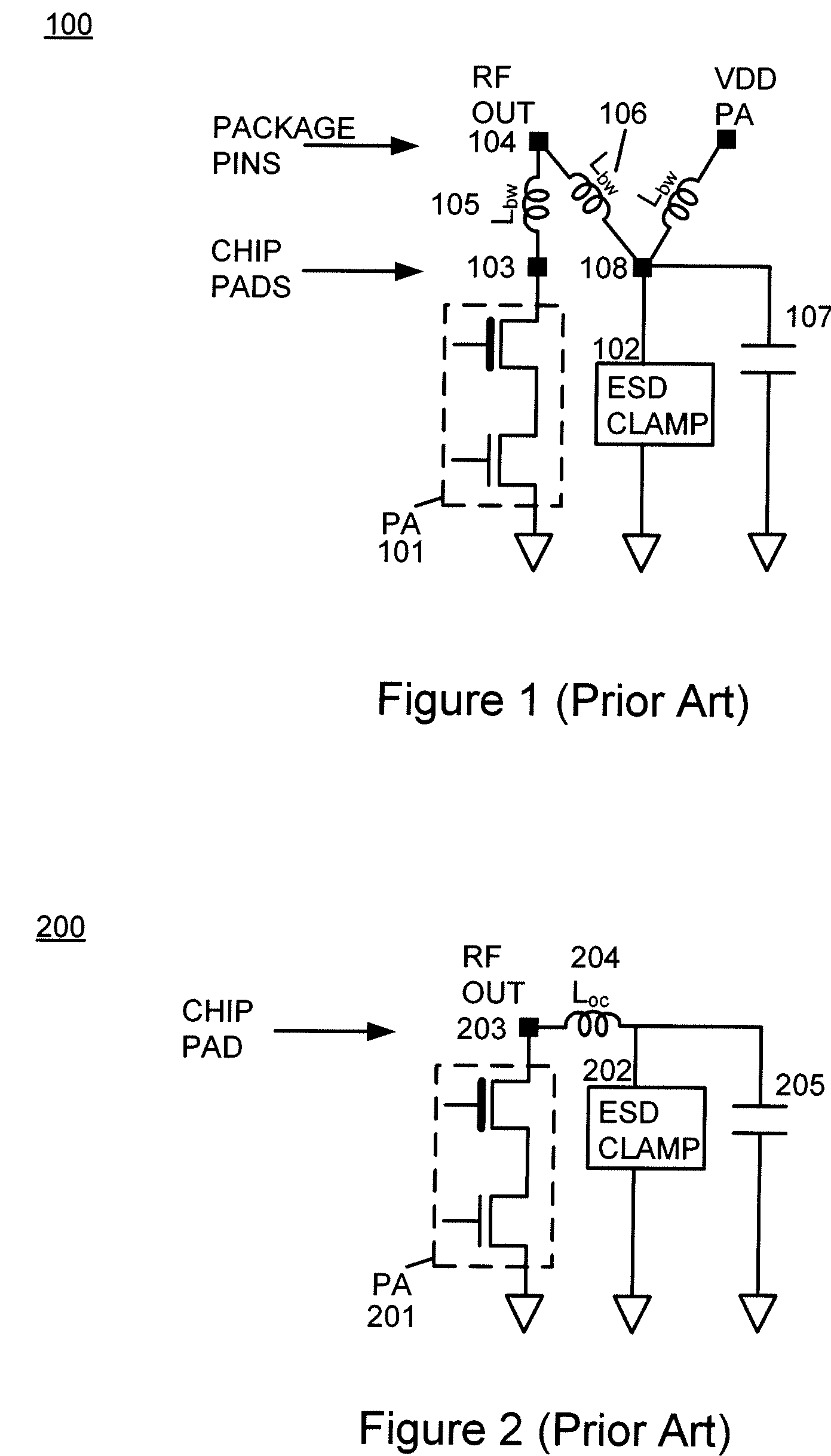
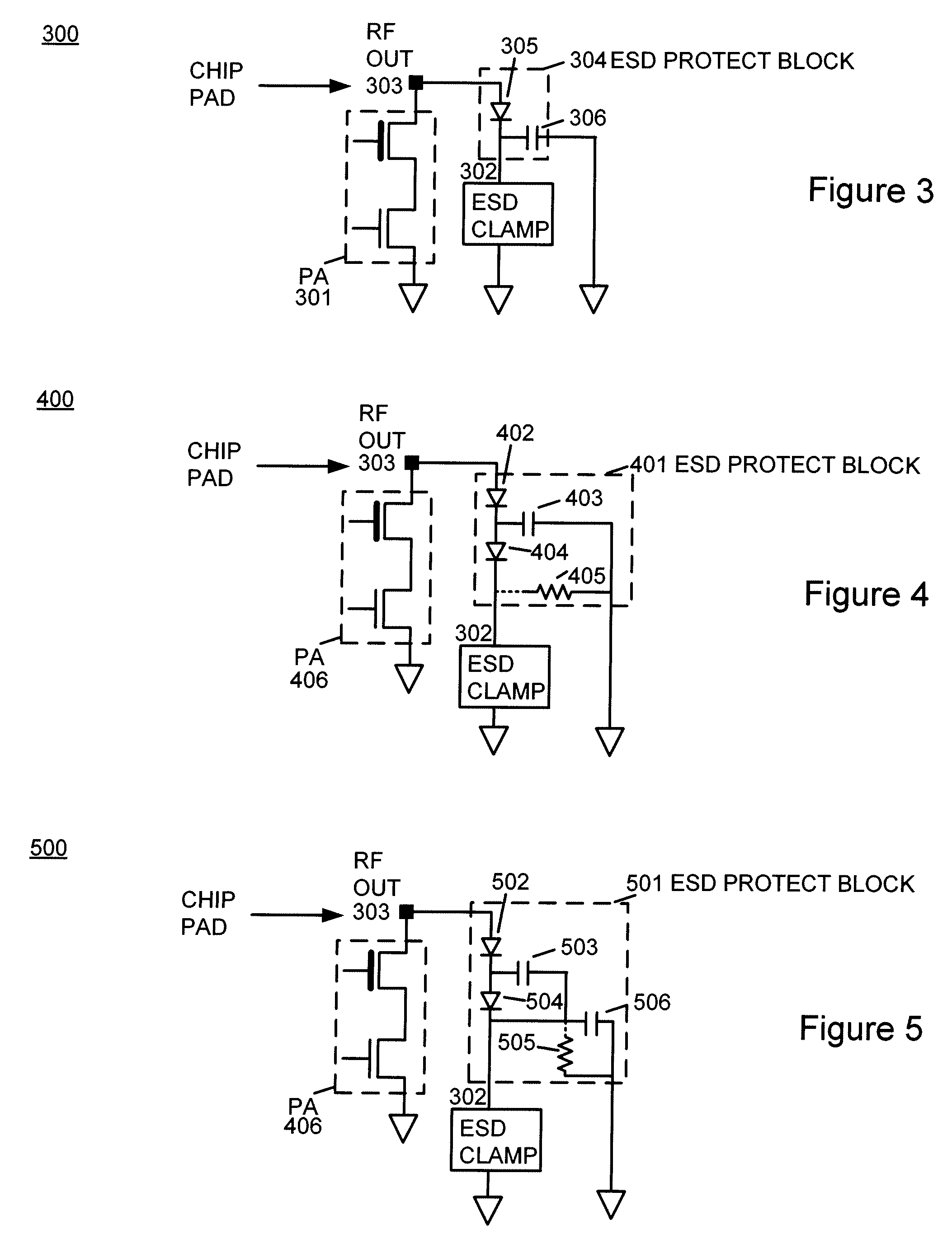
[0016]FIG. 3 illustrates one embodiment of an ESD protected integrated circuit 300 for a CMOS power amplifier (PA) 301 in a package without bond wires. A high voltage output signal from the PA 301 couples to an on chip pad 303 that couples to a package bump (not shown) without intervening bond wires. An ESD protect block 304, built from a diode 305 and a capacitor 306, couples between the chip pad 303 and an ESD clamp circuit 302, thereby protecting the ESD clamp circuit 302 from the high voltages generated by the PA 301, while simultaneously isolating the load of the ESD clamp circuit 302 from the PA 301.

[0017]When the PA 301 transmits an output signal, the voltage at the terminal of the capacitor 306 connected to a cathode of the diode 305 charges up to Vpeak,1-Vdiode,on; where Vpeak,1 of the output signal from the PA 301 may typically reach twice the supply voltage used for the PA 301, and Vdode,on equals approximately 0.7V. Once the capacitor 306 has charged up, the diode 305 op...


PUM


Abstract

An apparatus and method for providing electrostatic discharge protection of a transmit integrated circuit including an ESD protect block coupled to an integrated circuit pad in a package without bond wires, and an ESD clamp circuit coupled between the ESD protect block and ground. During transmission, one or more capacitors within the ESD protect block may charge up to various levels near the peak transmit voltage, which reverse biases one or more diodes in the ESD protect block, thereby buffering the transmit circuit from the capacitive load of the ESD clamp circuit. The ESD protect block may prevent the ESD clamp circuit from activating due to the high peak voltages output from the transmit circuit. An embodiment of the ESD protect block may apply particularly to transmit power amplifier circuits in which the output signal peaks at twice the supply voltage. In one embodiment applicable for lower voltage CMOS processes, the ESD protect block includes a diode and a capacitor. In another embodiment applicable for higher voltage CMOS processes, the ESD protect block includes two diodes, one or two capacitors, and an optional resistor.

Description

BACKGROUND OF THE INVENTION[0001]1. Field of the Invention[0002]Embodiments of the present invention generally relate to electrostatic discharge (ESD) protection, and more particularly to ESD protection of power amplifier integrated circuits.[0003]2. Description of the Related Art[0004]Electrostatic discharge (ESD) occurs when a static charge builds up in a human operator or machine and then through contact produces a large current in an integrated circuit in a short period of time. ESD may damage an unprotected complementary metal oxide semiconductor (CMOS) integrated circuit, and shrinking CMOS process technologies result in structures more susceptible to ESD damage. At the same time, increasing signaling rates of high speed communications systems require strict control of signal distortion to ensure adequate performance. A well designed ESD protection circuit should not alter significantly a transmit signal or a receive signal passing through the node the circuit protects.[0005]A...

Claims


Application Information

Patent Timeline
Patent Type & Authority Patents(United States)
IPC IPC(8): H02H3/20H02H3/22
CPCH01L27/0251H03F1/523H03F3/195H03F2200/444
Inventor TERROVITS, MANOLIS
Owner QUALCOMM INC
Why Eureka
Try Eureka