

Circuit board with high thermal conductivity and method for manufacturing the same
a technology of circuit boards and thermal conductivity, applied in the field of circuit boards, can solve the problems of reduced circuit board size, difficult heat dissipation, and disadvantages of ceramic materials as multi-layer substrates, and achieve the effect of improving the thermal conductivity of circuit boards and facilitating rapid heat dissipation of heat generated by semiconductor devices
- Summary
- Abstract
- Description
- Claims
- Application Information
AI Technical Summary
Benefits of technology
Problems solved by technology
Method used
Image

Examples
embodiment 1
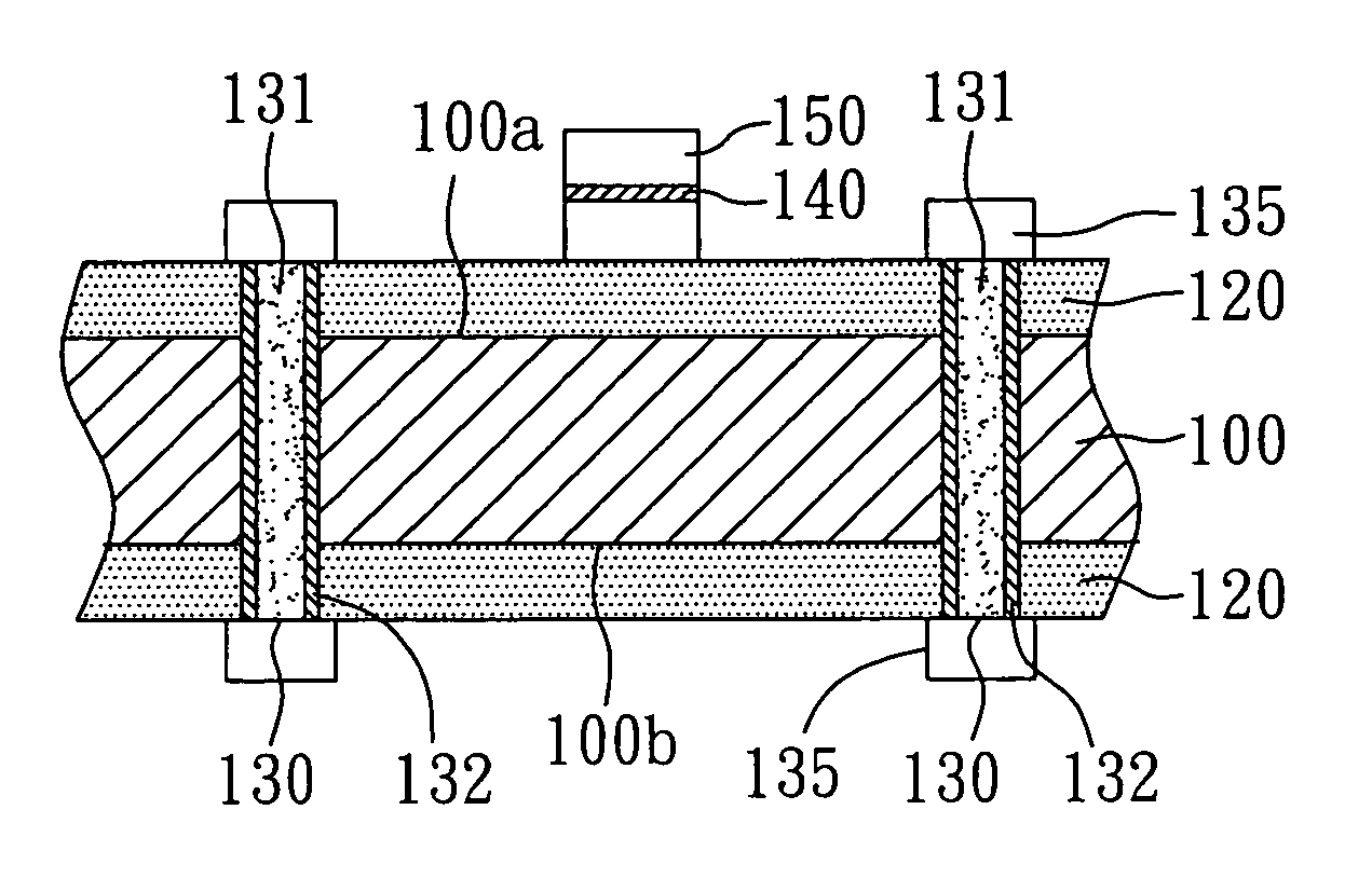
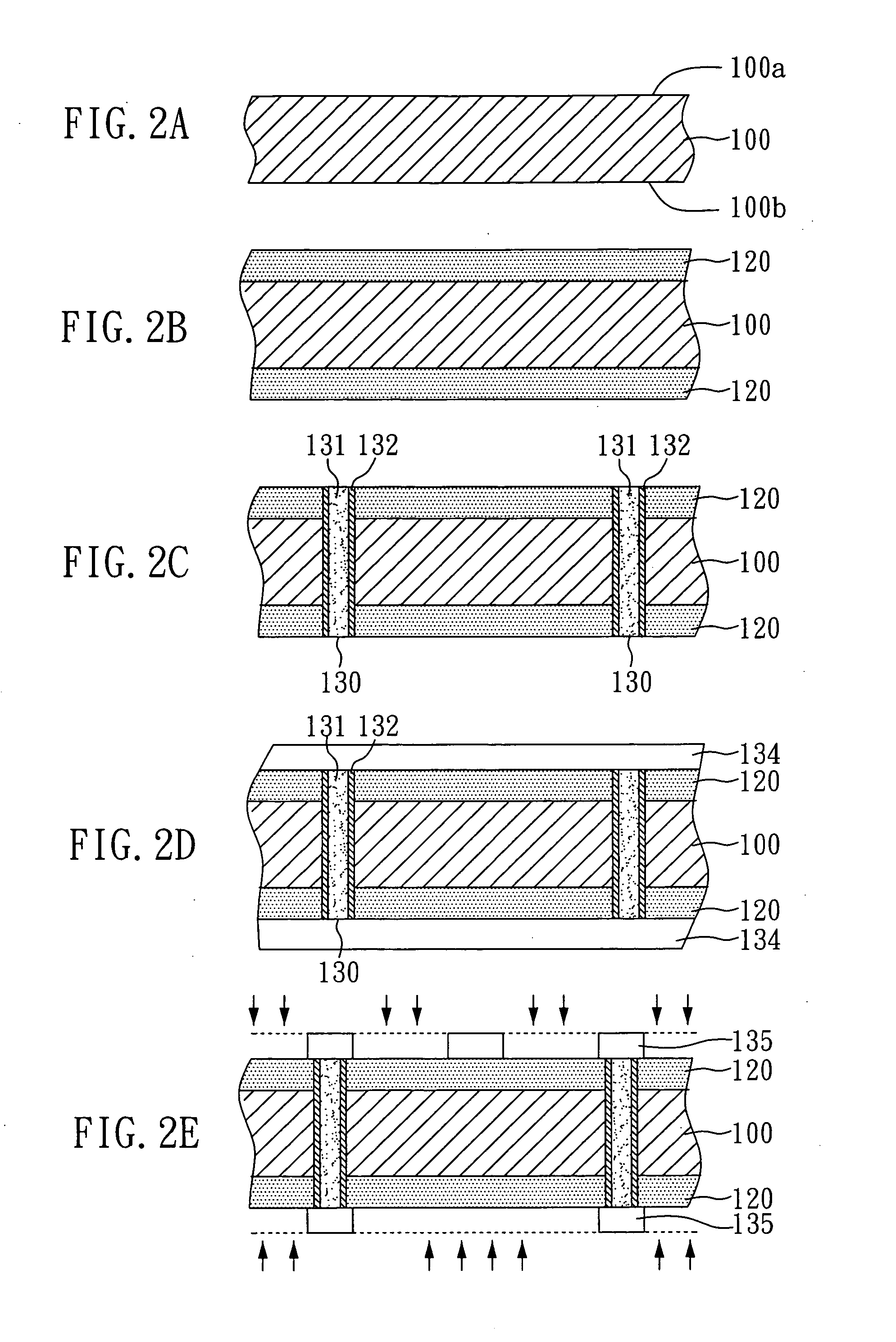
[0037]With reference to FIG. 1, there is shown a cross-sectional view of a circuit board according to an embodiment of the present invention. The circuit board of the present invention comprises: a substrate 100, a thermal conductive insulating layers 120, and a patterned electrical conductive layer 135. Herein, the thermal conductive insulating layers 120 are respectively formed on an upper surface 100a and a lower surface 100b of the substrate 100, and the patterned electrical conductive layer 135 is disposed on the surfaces of the thermal conductive insulating layers 120. The patterned electrical conductive layer 135 can be applied to electrically connect to other electronic components. For example, the patterned electrical conductive layer 135 is electrically connected to electronic components through wires. The material of the patterned electrical conductive layer 135 comprises materials with electrical conductivity, such as Cr, Cu, or Ag. Additionally, in the present embodimen...
embodiment 2
[0045]With reference to FIG. 3, there is shown a cross-sectional view of a circuit board according to another embodiment of the present invention. The circuit board and the method for manufacturing the same of the present embodiment are similar to those of the aforementioned embodiment. In comparison to the circuit board illustrated in the aforementioned embodiment, the circuit board of the present embodiment further comprises a plurality of ceramic layers 110 respectively formed on the upper surface and the lower surface of the substrate 100, and thermal conductive insulating layers 120 are formed on the surface of the ceramic layers 110. The material of the ceramic layers 110 is unlimited. Preferably, the material of the ceramic layers 110 is oxide, nitride, or boride. It should be noted that the method used for forming the ceramic layers 110 depends upon the material of the substrate 100. In the present embodiment, when the substrate 100 is a metal substrate, the ceramic layers 1...
PUM
| Property | Measurement | Unit |
|---|---|---|
| thickness | aaaaa | aaaaa |
| thickness | aaaaa | aaaaa |
| thickness | aaaaa | aaaaa |
Abstract
Description
Claims
Application Information